

Compositions for processing of semiconductor substrates
- Summary
- Abstract
- Description
- Claims
- Application Information
AI Technical Summary
Benefits of technology
Problems solved by technology
Method used
Image

Examples
example 1
[0225]PCMP Cleaning Compositions were employed for post CMP cleaning of PCMP 854 wafers (wafers fabricated with the Sematech 854 wafer pattern). The wafers had dried slurry and other PCMP residues on their surface. The wafer in each instance was cleaned on a spin / spray tool with solutions diluted 30:1 (1 part of the composition and 30 parts deionized water as diluent) for 1 minute at 22° C., 100 rpm with a 30 second DI water rinse and spin dry. Pre- and post-cleaning analysis was carried out using a Nanoscope IIIa atomic force microscope.
[0226]The cleaning efficacy was rated by the reduction of objects on the substrate. The particles on the sample substrates were registered as a range of pixels from 231-235 intensity. A Sigma Scan Pro histogram was applied to filter these pixels and count the number of particles. The particle reduction was calculated as:
CleaningEfficacy=(NumberofPreCleanObjects-NumberofPostCleanObjects)(NumberofPreCleanObjects)×100
[0227]Table 1 below contains the PC...
example 2
[0229]Surface Preparation for Cobalt Plating Compositions in accordance with the invention were employed for surface preparation of microelectronic device wafers, viz., Cu / TEOS 854 wafers (TEOS=tetraethylorthosilicate), for subsequent cobalt plating. The compositions were diluted 40:1 (1 part of the composition and 40 parts deionized water as diluent) and applied to the wafers by static immersion for 30 seconds at 22° C. with a DI water rinse prior to cobalt plating. Analysis was carried out using a JEOL scanning electron microscope (SEM).
[0230]A first set of compositions was evaluated, each containing 0.5 wt % tetramethylammonium hydroxide, 1 wt % monoethanolamine, 21 wt %, triethanolamine, 1.5-2.0 wt % complexing agent and balance DI water, against a corresponding control composition containing no complexing agent (composition AV). The complexing agents evaluated in this test were lactic acid (composition AW), oxalic acid (composition AX), and citric acid (composition AY). The con...
example 3
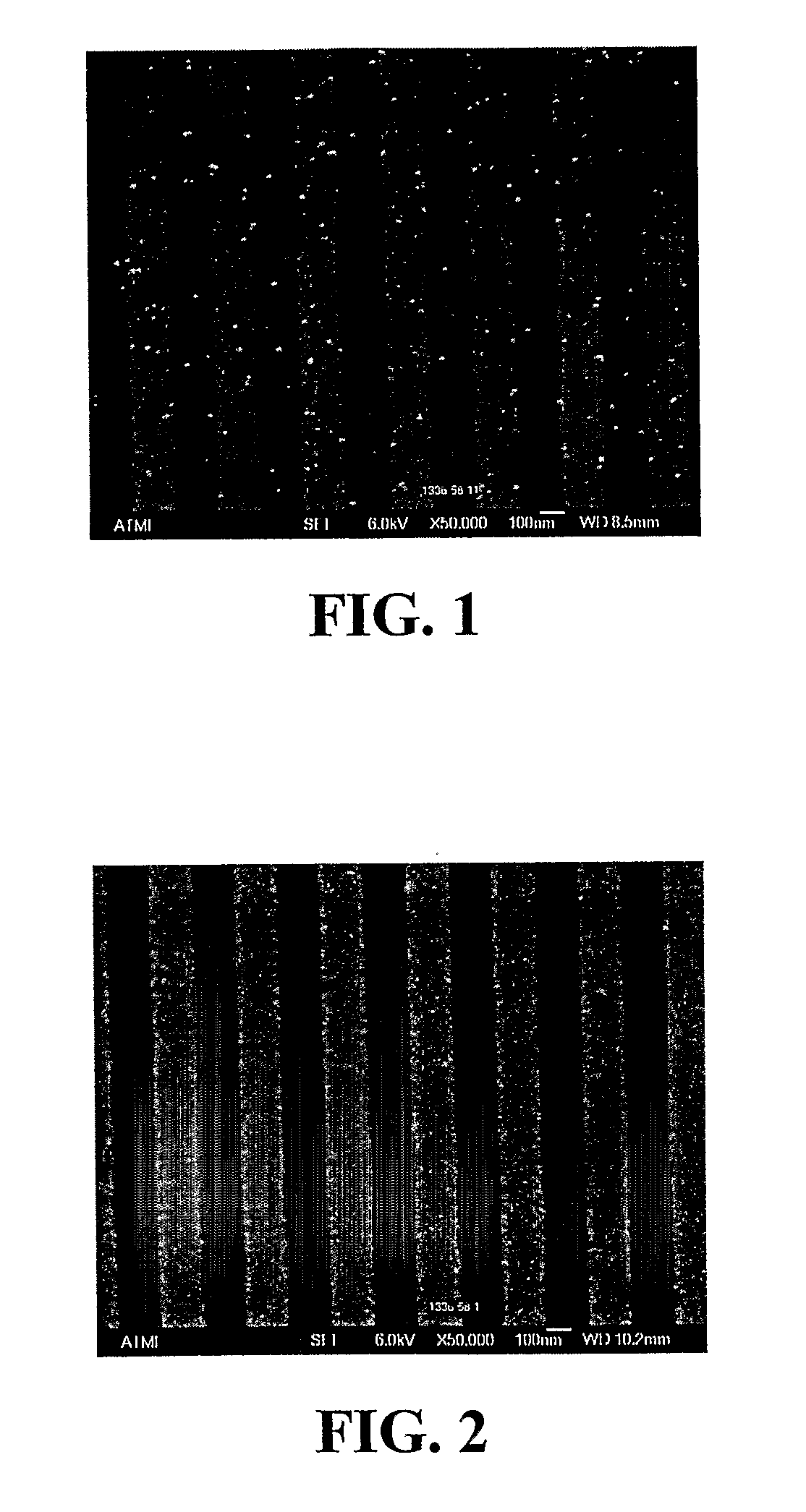
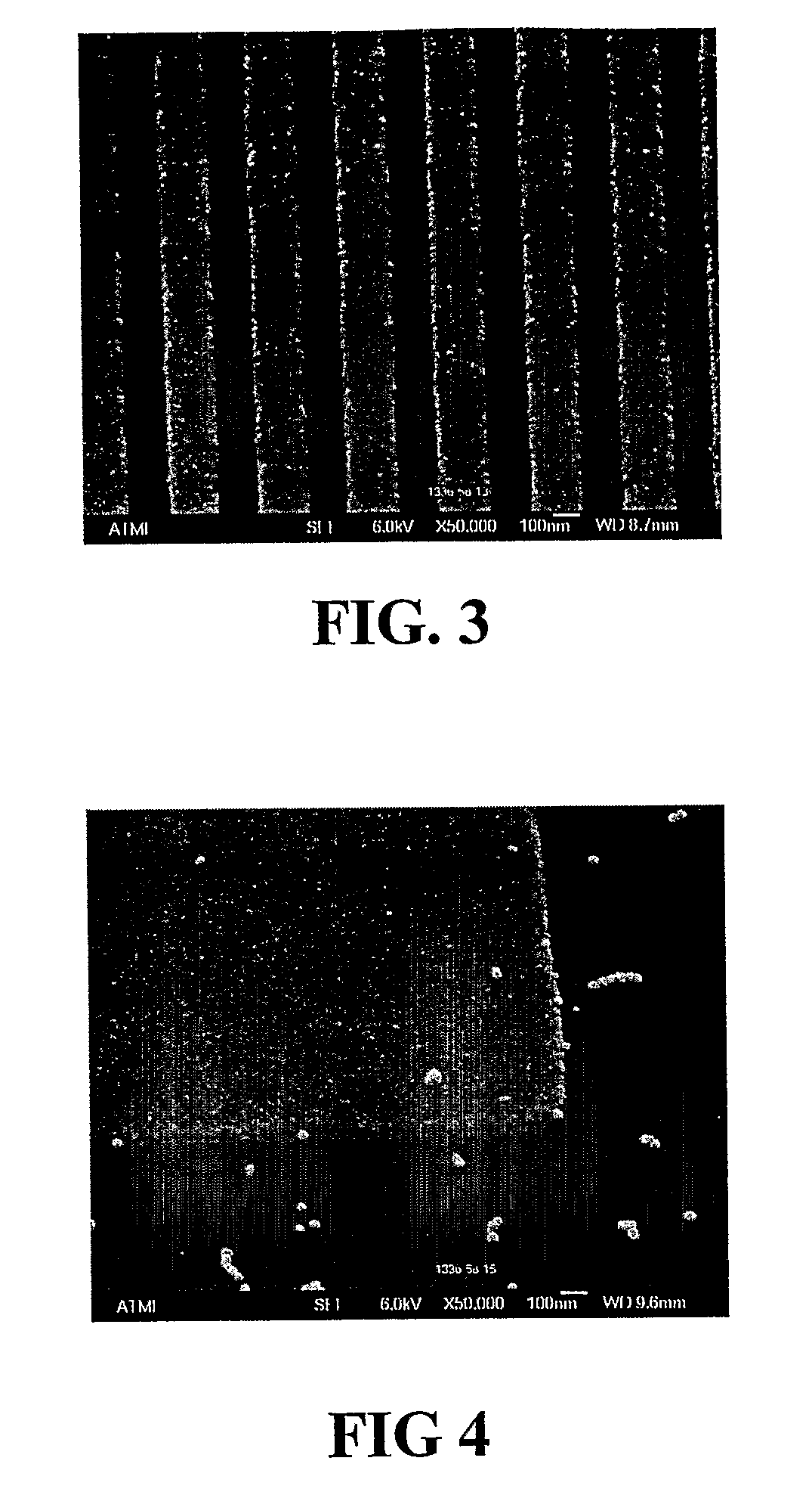
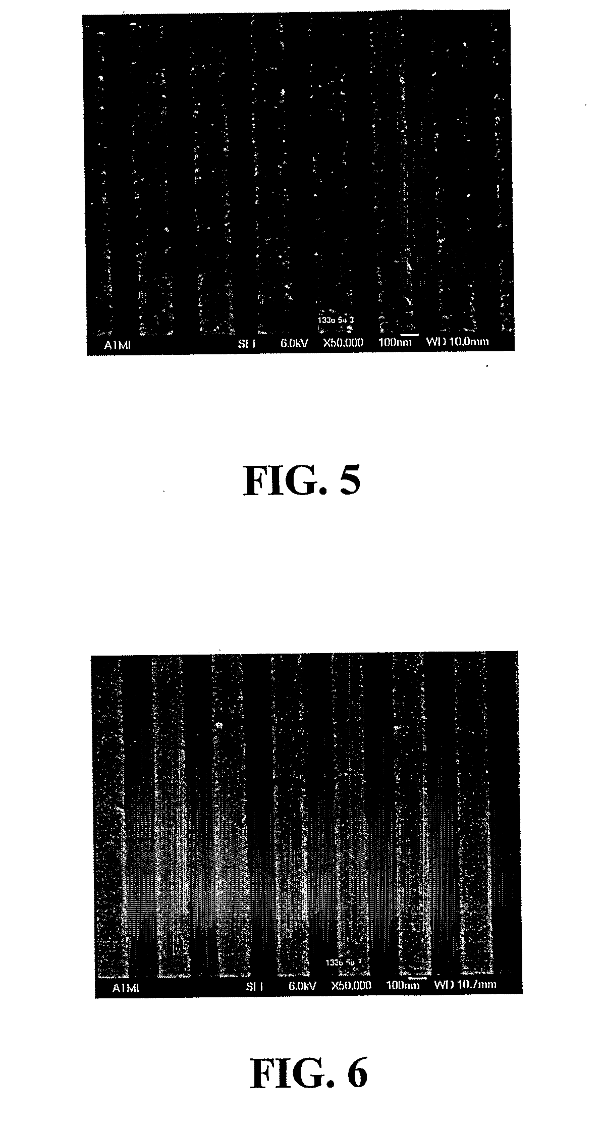
[0234]Copper Attack of 0.18 μm Lines on a Device Test Pattern
[0235]The compositions as described above were tested for copper attack on 854 patterned Cu / TEOS wafers (TEOS=tetraethylorthosilicate). Wafer sections were dipped into solutions diluted 40:1 (1 part of the composition and 40 parts deionized water as diluent), at 22° C. for 5 minutes. The 0.18 μm lines were analyzed for copper etching by AFM to determine changes in line height and etch rate was measured, in Angstroms per minute. The data are set out in Table 4 below.
TABLE 4Copper Attack on 0.18 μm Lines, as Determined by Change in LineHeight, in Angstroms (A), and Measured Etch Rate (ER), in AngstromsPer Minute (A / min)FormulationDelta LineER(40:1)Height (A)(A / min)AA132.7BC40.9BD91.8BE3.90.8BF2.90.6BG7.91.6BH8.11.6BI6.21.2BJ11.82.4BK9.41.9BL12.52.5BM6.41.3BN3.00.6BO2.10.4BP7.71.5BQ3.00.6AZ3.90.8BR3.50.7BA2.50.5AW3.30.7BS00AX1.20.2
[0236]The data in Table 4 show low levels of attack on the 0.18 μm copper lines, with etch rates...
PUM
| Property | Measurement | Unit |
|---|---|---|
| Fraction | aaaaa | aaaaa |
| Fraction | aaaaa | aaaaa |
| Fraction | aaaaa | aaaaa |
Abstract
Description
Claims
Application Information