Device and method for analyzing a sample

a sample and device technology, applied in the field of sample device and method, can solve the problems of samples being damaged, disadvantageous in some applications, and gallium being used

Active Publication Date: 2010-03-11
CARL ZEISS SMT GMBH
View PDF10 Cites 38 Cited by
  • Summary
  • Abstract
  • Description
  • Claims
  • Application Information

AI Technical Summary

Benefits of technology

[0014]In a further embodiment, the method according to the system described herein may be combined with other measuring methods. In particular, it is provided that, when the electron beam hits the sample, cathodoluminescence light exiting the sample may be additionally detected. Alternatively or additionally, the sample may be examined using energy-dispersive X-ray spectroscopy (EDX), and/or the sample may be examined using wavelength-dispersive X-ray spectroscopy (WDX). Another embodiment provides that, additionally or alternatively to the above-mentioned measuring methods, the sample may be examined using secondary ion mass spectrometry (SIMS). Moreover, it is alternatively or additionally provided that the sample may be examined with the aid of an analysis of secondary electrons (i.e., electrons emitted by the sample, also known by the abbreviation SE) and/or of electrons backscattered from the sample (backscattered electrons, also known by the abbreviation BSE). The combination of at least one of the above-mentioned mea

Problems solved by technology

The use of gallium may be disadvantageous in some applications.
In the case of some sampl

Method used


Image

  • Device and method for analyzing a sample
  • Device and method for analyzing a sample
  • Device and method for analyzing a sample

Examples


Embodiment Construction

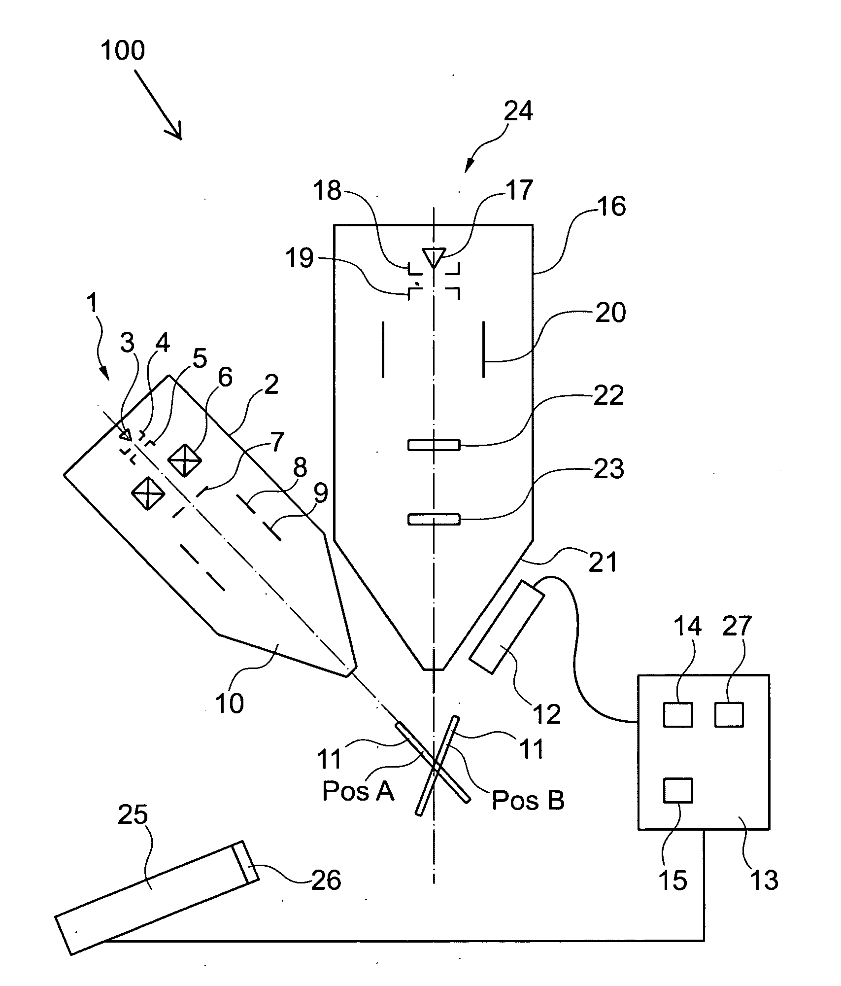
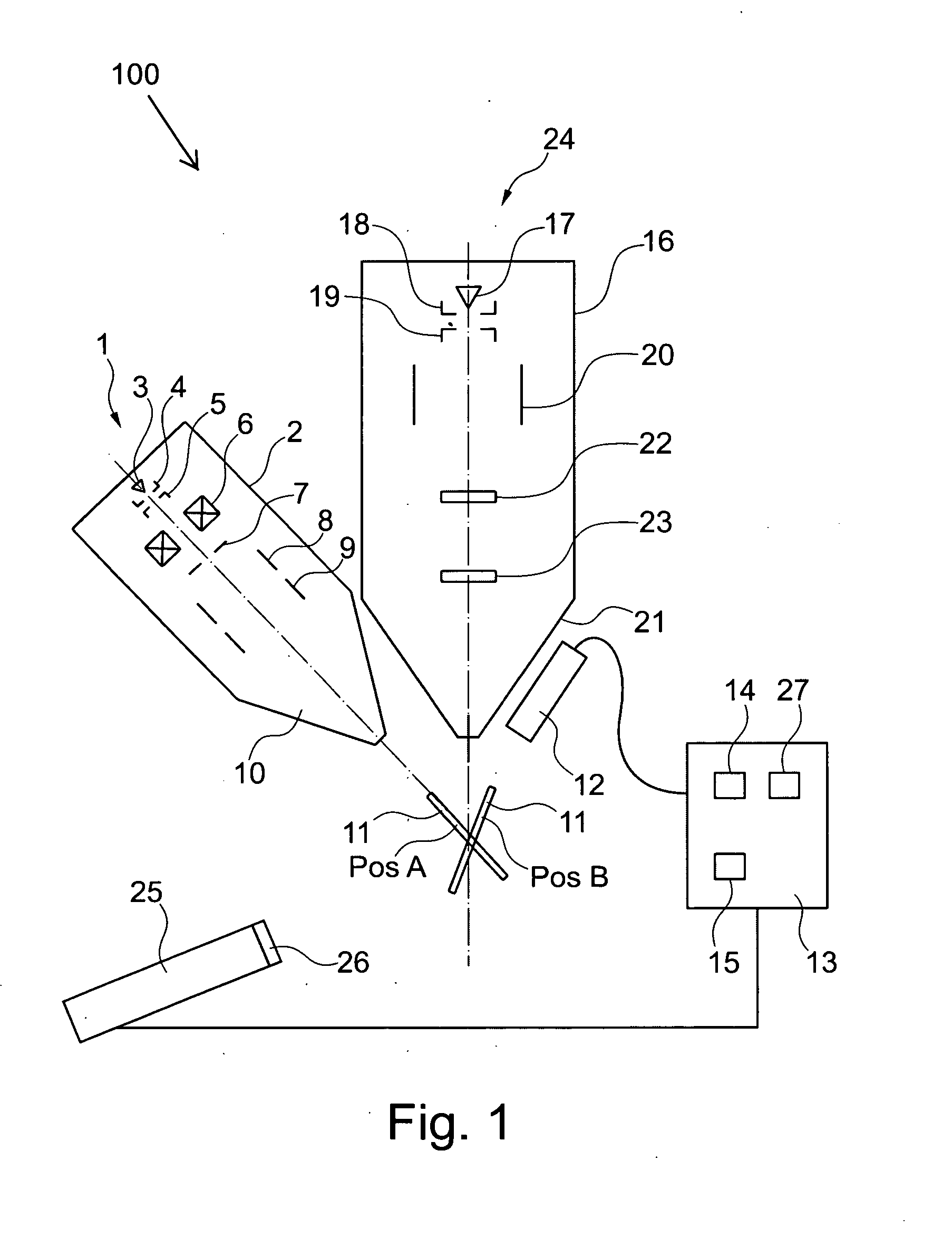
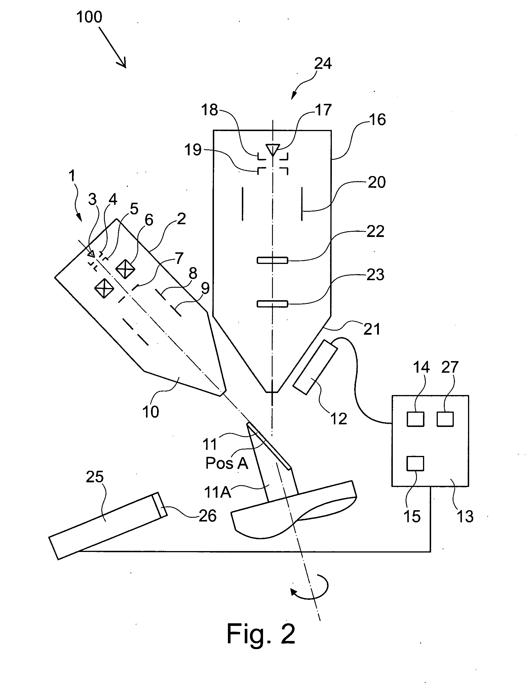
[0028]FIG. 1 shows a schematic representation of a particle beam device 100 which has an ion beam device 1 and an electron beam device 24 according to an embodiment of the system described herein. The method according to the system described herein, which is discussed in greater detail elsewhere herein, may be carried out using the described and illustrated particle beam device 100.

[0029]The ion beam device 1 may have an ion beam column 2 in which numerous units of the ion beam device 1 may be situated. In particular, an ion source 3 may be situated in the ion beam column 2. The ion source 3 may generate ions which form an ion beam in the ion beam column 2. The ion source 3 may generate a variety of ions of different masses and / or numbers of elementary charges. In the embodiment illustrated in FIG. 1, it is provided, for example, that the variety of ions has or contains ions of a plurality of the following elements: silicon (Si), chromium (Cr), iron (Fe), cobalt (Co), nickel (Ni), g...


PUM


Abstract

A device and method for analyzing a sample, in particular a sample which contains low-density materials, is provided. Ions of a predefined mass and/or a predefined elementary charge are selected from a plurality of ions. The selected ions are directed onto the sample for sample preparation. An electron beam is then directed onto the prepared sample and a spatial distribution of scattered electrons is measured.

Description

TECHNICAL FIELD[0001]This application relates to a device and method for analyzing a sample, in particular a sample which contains low-density materials.BACKGROUND OF THE INVENTION[0002]The use of an ion beam column for repairing semiconductor masks is known from the prior art. The ion beam column has an ion source, which provides a plurality of ions of different suitable elements, which have different ion masses. The ions are combined in an ion beam and directed toward a semiconductor mask to be repaired. A desired type of ions is selected on the basis of their mass with the help of a filter which provides both an electric field and a magnetic field. Ultimately only these selected ions are focused on the semiconductor mask as an ion beam. Due to an interaction of the ion beam incident on the semiconductor mask with the material of the semiconductor mask, interaction particles are generated, in particular secondary electrons or secondary ions, which are emitted from the semiconducto...

Claims


Application Information

Patent Timeline
IPC IPC(8): G01N23/203H01J49/26G01N23/225H01J27/02
CPCG01N23/2251H01J37/28H01J37/3005H01J37/3056H01J2237/31749H01J2237/2445H01J2237/24485H01J2237/2807H01J2237/31745H01J2237/2442
Inventor ZEILE, ULRIKE
Owner CARL ZEISS SMT GMBH
Why Eureka
Try Eureka