Structure and method to fabricate high performance MTJ devices for spin-transfer torque (STT)-RAM

a technology of spin-transfer torque and high-performance mtj, which is applied in the manufacture of inductance/transformer/magnet, magnetic body, instruments, etc., can solve the problems of affecting the magnetic moment direction, and introducing statistical difficulties in the read process. , to achieve the effect of facilitating the magnetization switching of the free layer and negatively affecting the tunnel barrier layer

Active Publication Date: 2010-03-18
TAIWAN SEMICON MFG CO LTD
View PDF9 Cites 60 Cited by
  • Summary
  • Abstract
  • Description
  • Claims
  • Application Information

AI Technical Summary

Benefits of technology

[0020]One objective of the present invention is to provide a MTJ for an STT-RAM that delivers a high dR/R of about 100% with a RA of less than about 15 ohm-μm2, a

Problems solved by technology

As the size of MRAM cells decreases, the use of external magnetic fields generated by current carrying lines to switch the magnetic moment direction becomes problematic.
Needless to say, the read process introduces some statistical difficulties associated with the variation of resistances of MTJ cells within an array.
If the a

Method used


Image

  • Structure and method to fabricate high performance MTJ devices for spin-transfer torque (STT)-RAM
  • Structure and method to fabricate high performance MTJ devices for spin-transfer torque (STT)-RAM
  • Structure and method to fabricate high performance MTJ devices for spin-transfer torque (STT)-RAM

Examples


Embodiment Construction

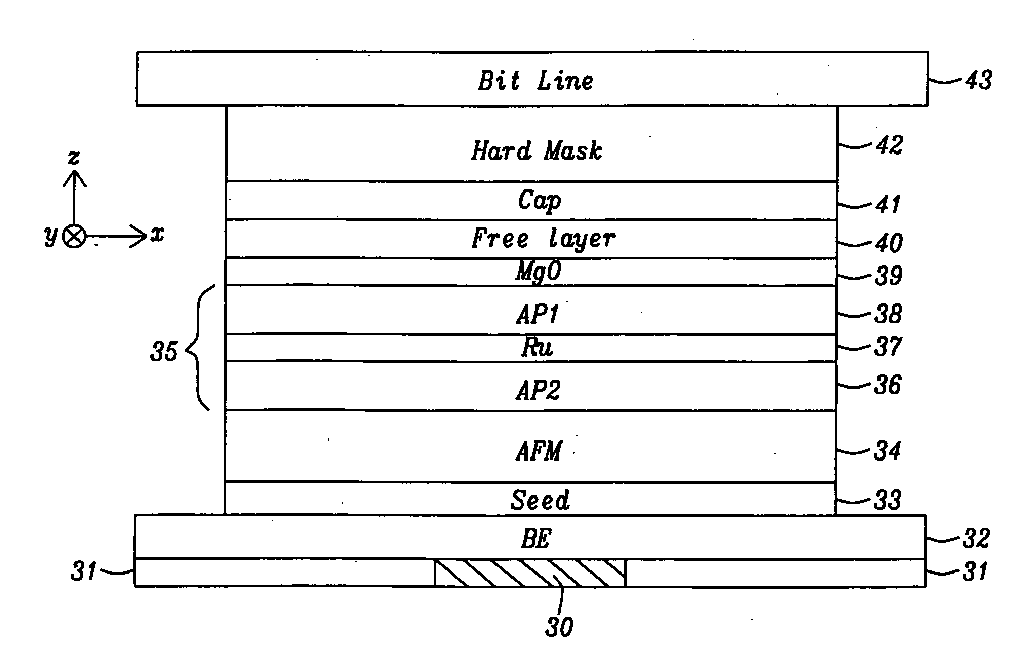
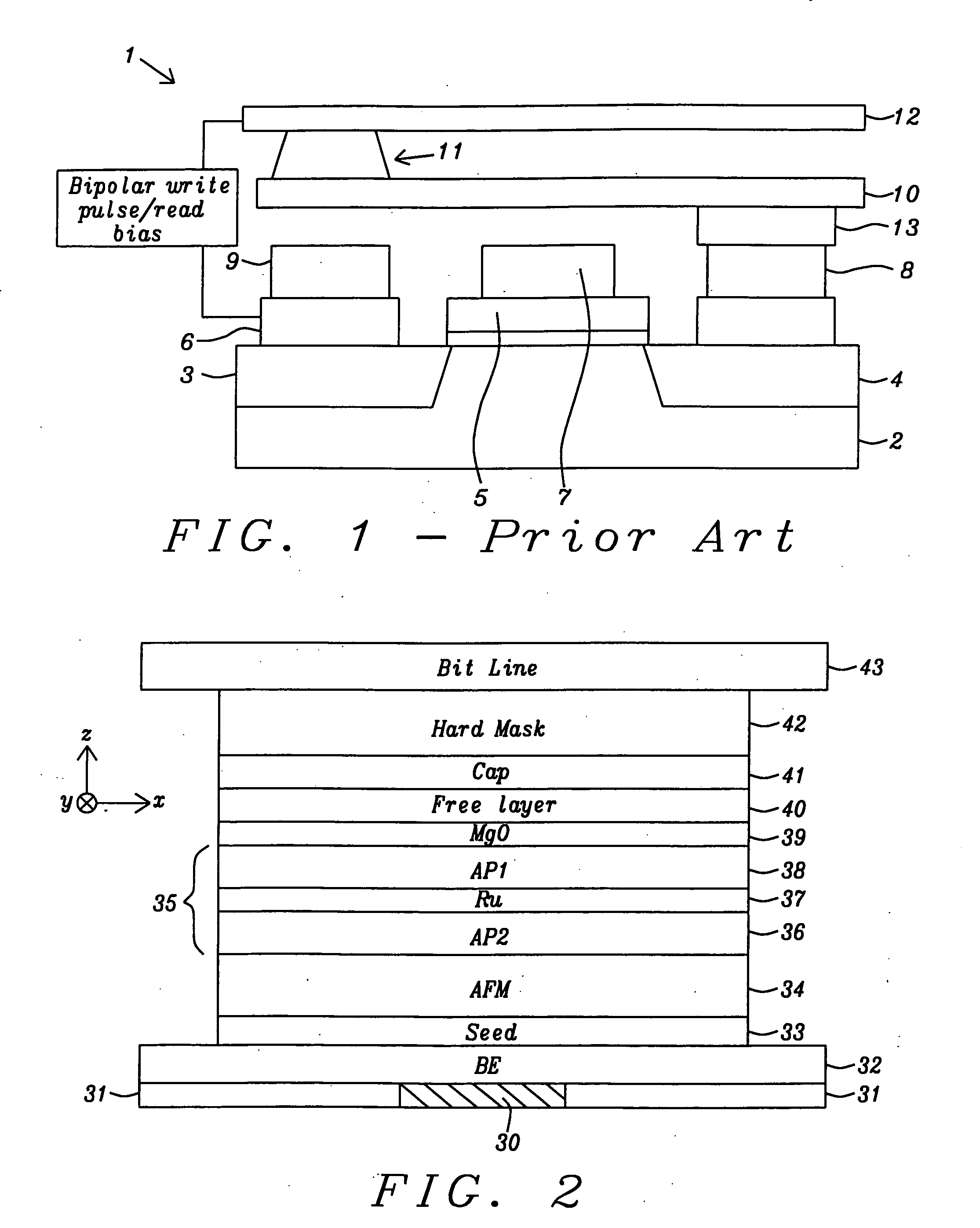
[0034]The present invention is a MTJ element (nanopillar) for an STT-RAM application that provides a combination of high dR / R, low RA, and low critical current density which is necessary for enhanced performance in high density STT-RAMs. The present invention also provides a fabrication sequence for a STT-RAM on an ultra high density scale. Drawings are provided by way of example and are not intended to limit the scope of the invention. Although the exemplary embodiment depicts a bottom spin valve configuration, the present invention also encompasses a top spin valve design as appreciated by those skilled in the art. A “top view” as described herein is defined as a viewpoint from a position above the plane of the substrate in the STT-RAM device.

[0035]Referring to FIG. 2, one embodiment of a MTJ according to the present invention is depicted. In particular, a MTJ comprised of layers 33-42 is formed between a bottom electrode 32 and a bit line 43 in an MRAM array (not shown). The bott...


PUM


Abstract

A STT-RAM MTJ is disclosed with a MgO tunnel barrier formed by a NOX process, a CoFeB/FeSiO/CoFeB composite free layer with a middle nanocurrent channel layer to minimize Jc0, and a Ru capping layer to enhance the spin scattering effect and increase dR/R. Good write margin is achieved by modifying the NOX process to afford a RA less than 10 ohm-μm2 and good read margin is realized with a dR/R of >100% by annealing at 330° C. or higher to form crystalline CoFeB free layers. The NCC thickness is maintained in the 6 to 10 Angstrom range to reduce Rp and avoid Fe(Si) granules from not having sufficient diameter to bridge the distance between upper and lower CoFeB layers. A FeSiO layer may be inserted below the Ru layer in the capping layer to prevent the Ru from causing a high damping constant in the upper CoFeB free layer.

Description

RELATED PATENT APPLICATIONS[0001]This application is related to the following: Docket #HMG07-042, Ser. No. 12 / 079,445, filing date Mar. 27, 2008; and Docket #HMG07-046 / 052, Ser. No. 12 / 082,155, filing date Apr. 9, 2008; both of which are assigned to a common assignee and are herein incorporated by reference in their entirety.FIELD OF THE INVENTION[0002]The invention relates to a high performance Magnetic Tunneling Junction (MTJ) element and a method for making the same, and in particular, to a spin transfer (Spin-RAM) device that achieves low switching current and high dR / R by incorporating a free layer having a FeCoB / FeSiO / FeCoB configuration in which the thinner, upper FeCoB layer is easier to switch than the lower, thicker FeCoB layer and the single MTJ functions like a dual spin filter (DSF).BACKGROUND OF THE INVENTION[0003]Magnetoresistive Random Access Memory (MRAM), based on the integration of silicon CMOS with MTJ technology, is a major emerging technology that is highly com...

Claims


Application Information

Patent Timeline
IPC IPC(8): H01L29/82H01L21/00
CPCB82Y25/00B82Y40/00H01F10/3254H01F10/3272H01F41/307H01F10/3259G11C11/161G11C11/1675H10N50/01H10N50/10
Inventor HORNG, CHENG T.TONG, RU-YINGTORNG, CHYU-JIUHWANG, PO-KANGBEACH, ROBERTKULA, WITOLD
Owner TAIWAN SEMICON MFG CO LTD
Why Eureka
Try Eureka