Display device

a display device and display technology, applied in the field of display devices, can solve the problems of increasing manufacturing costs, and achieve the effects of reducing manufacturing costs, excellent electrical properties, and high reliability

Active Publication Date: 2010-04-08
SEMICON ENERGY LAB CO LTD
View PDF11 Cites 159 Cited by
  • Summary
  • Abstract
  • Description
  • Claims
  • Application Information

AI Technical Summary

Benefits of technology

[0029]A thin film transistor in which an oxide semiconductor is used in a gate line driver circuit or source line driver circuit, whereby manufacturing costs can be reduced. Moreover, a gate electrode of the thin film transistor used for the driver circuit is directly connected to a source wiring or a drain wiring, whereby a display device in which the number of contact holes can be reduced and an area occupied by the driver circuit is reduced can be provided.
[0030]Therefore, according to an embodiment of the present invention, a display device having excellent electrical properties and high reliability can be provided at low costs.

Problems solved by technology

Due to the increase in the numbers of gate lines and signal lines, it is difficult to mount an IC chip having a driver circuit for driving the gate and signal lines by bonding or the like, which causes an increase in manufacturing costs.

Method used


Image

  • Display device
  • Display device
  • Display device

Examples


embodiment 1

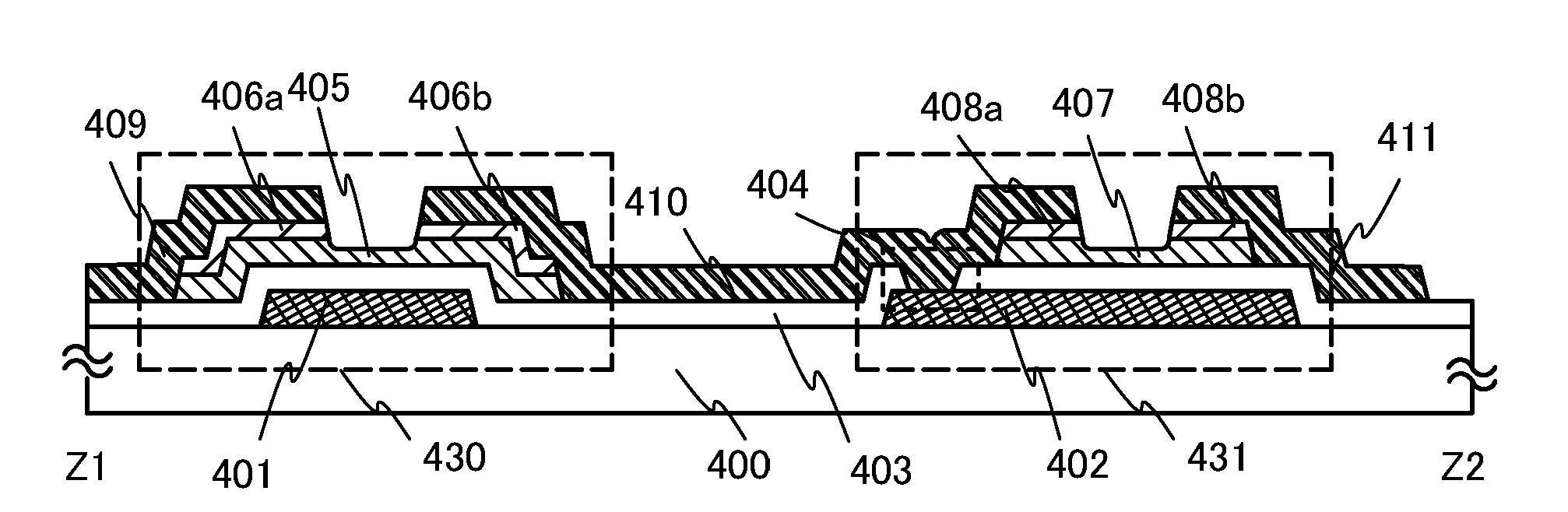
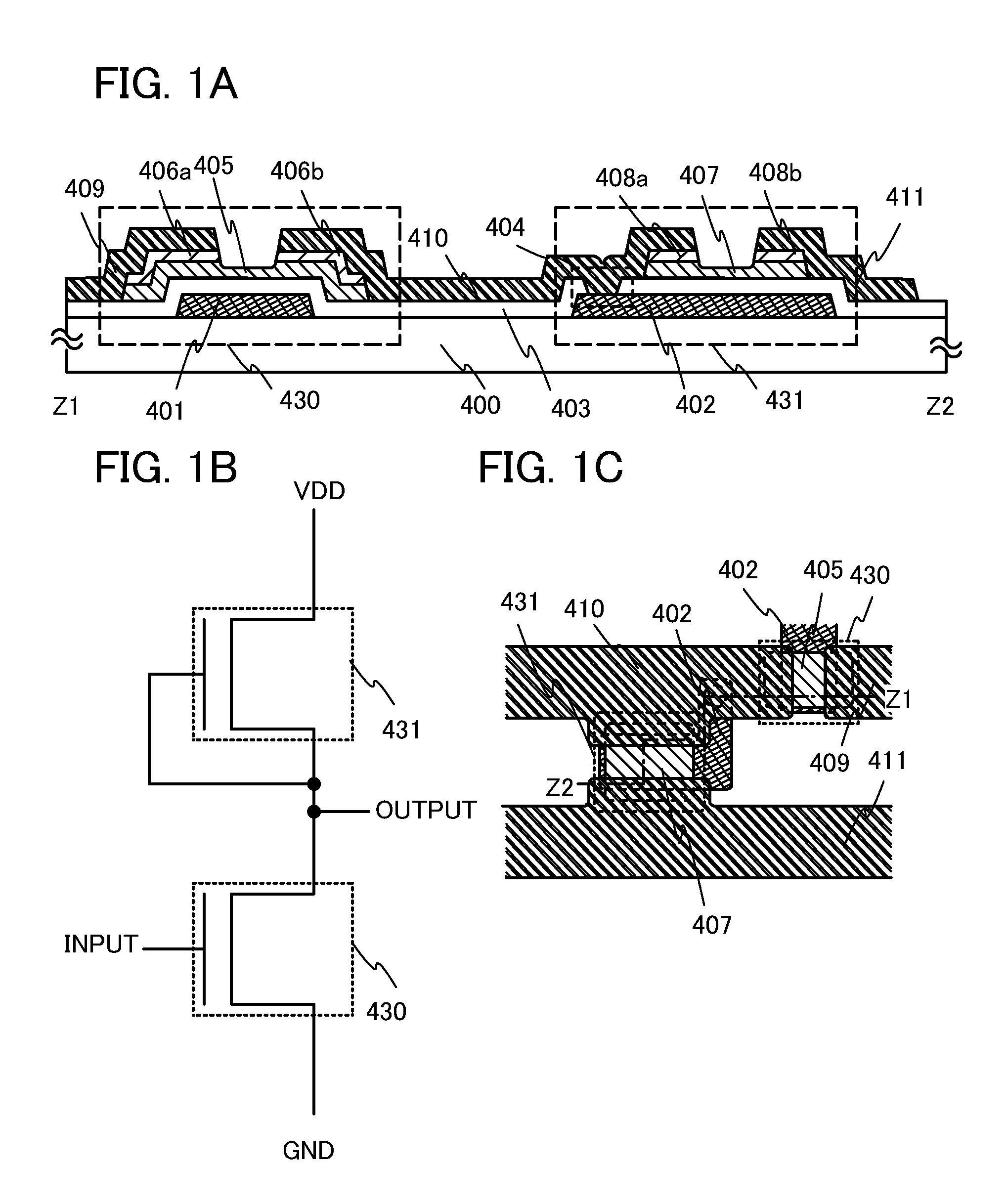
[0062]In this embodiment, an embodiment of the present invention will be described based on an example in which an inverter circuit is formed using two n-channel thin film transistors.

[0063]A driver circuit for driving a pixel portion is formed using an inverter circuit, a capacitor, a resistor, and the like. When two n-channel TFTs are combined to form an inverter circuit, there are two types of combinations: a combination of an enhancement type transistor and a depletion type transistor (hereinafter, a circuit formed by such a combination is referred to as an “EDMOS circuit”) and a combination of enhancement type TFTs (hereinafter, a circuit formed by such a combination is referred to as an “EEMOS circuit”). Note that when the threshold voltage of the n-channel TFT is positive, the n-channel TFT is defined as an enhancement type transistor, while when the threshold voltage of the n-channel TFT is negative, the n-channel TFT is defined as a depletion type transistor, and this speci...

embodiment 2

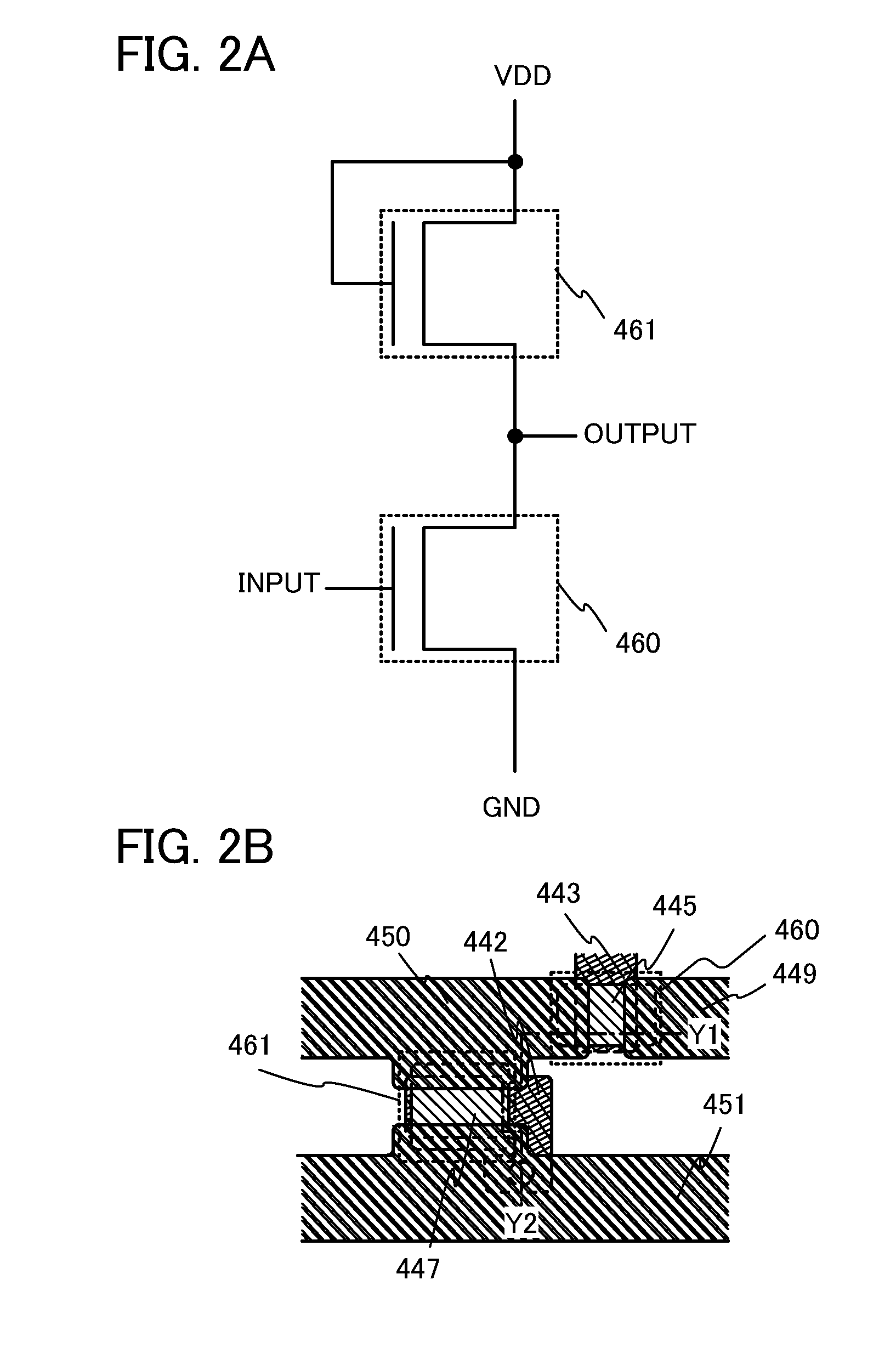
[0079]Although the example of the EDMOS circuit is described in Embodiment 1, an equivalent circuit of an EEMOS circuit is illustrated in FIG. 2A in this embodiment. In the equivalent circuit illustrated in FIG. 2A, a driver circuit can be formed in either case: a case where a first thin film transistor 460 and a second thin film transistor 461 are both enhancement type n-channel transistors, or a case where the first thin film transistor 460 is an enhancement type n-channel transistor and the second thin film transistor 461 is a depletion n-channel transistor.

[0080]It can be said that it is preferable to use the circuit configuration illustrated in FIG. 2A in which enhancement type n-channel transistors of the same type are combined for the driver circuit. This is because in that case, a transistor used for a pixel portion is also formed of an enhancement type n-channel transistor which is the same type as that used for the driver circuit, and therefore the number of manufacturing ...

embodiment 3

[0093]In this embodiment, an example of a manufacturing process of an inverter circuit which is different from the process described in Embodiment 2 will be described using FIGS. 4A to 4C.

[0094]A first conductive film is formed over the substrate 440 by a sputtering method and the first conductive film is etched as selected using a first photomask to form the first gate electrode 441 and the second gate electrode 442. Next, the gate insulating layer 443 for covering the first gate electrode 441 and the second gate electrode 442 is formed by a plasma CVD method or a sputtering method.

[0095]Next, an oxide semiconductor film is formed by a sputtering method, and an n+-type layer is formed thereover.

[0096]Next, the oxide semiconductor film and the n+-type layer are etched as selected using the second photomask. Thus, an oxide semiconductor film 454 and an n+-type layer 455 are formed which are overlapped with the first gate electrode 441 with the gate insulating layer 443 interposed the...


PUM


Abstract

With an increase in the definition of a display device, the number of pixels is increased, and thus the numbers of gate lines and signal lines are increased. Due to the increase in the numbers of gate lines and signal lines, it is difficult to mount an IC chip having a driver circuit for driving the gate and signal lines by bonding or the like, which causes an increase in manufacturing costs. A pixel portion and a driver circuit for driving the pixel portion are formed over one substrate. At least a part of the driver circuit is formed using an inverted staggered thin film transistor in which an oxide semiconductor is used. The driver circuit as well as the pixel portion is provided over the same substrate, whereby manufacturing costs are reduced.

Description

TECHNICAL FIELD[0001]The present invention relates to a display device in which an oxide semiconductor is used and a method for manufacturing the display device.BACKGROUND ART[0002]As typically seen in a liquid crystal display device, a thin film transistor formed over a flat plate such as a glass substrate is manufactured using amorphous silicon or polycrystalline silicon. Thin film transistors manufactured using amorphous silicon has low field effect mobility, but can be formed over a larger glass substrate. In contrast, thin film transistors manufactured using crystalline silicon has high field effect mobility, but due to a crystallization step such as laser annealing, the transistors are not always suitable for being formed over a larger glass substrate.[0003]In view of the foregoing, attention has been drawn to a technique for by which a thin film transistor is manufactured using an oxide semiconductor and such a transistor is applied to an electronic appliance or an optical de...

Claims


Application Information

Patent Timeline
Patent Type & Authority Applications(United States)
IPC IPC(8): H01L33/00
CPCH01L27/1225H01L27/124H01L29/7869H01L27/1214H10K59/1213H10K59/131H10K59/90H10K2102/351G02F1/13624
Inventor YAMAZAKI, SHUNPEIAKIMOTO, KENGOUMEZAKI, ATSUSHI
Owner SEMICON ENERGY LAB CO LTD
Why Eureka
Try Eureka