

Inverter manufacturing method and inverter
a manufacturing method and inverter technology, applied in the field of inverters, can solve the problems of inability to use constitution, difficult to inexpensively manufacture tft digital circuits, and inability to disclose concrete methods in documents, etc., to achieve the effect of reducing production costs, facilitating manufacture, and reducing production costs
- Summary
- Abstract
- Description
- Claims
- Application Information
AI Technical Summary
Benefits of technology
Problems solved by technology
Method used
Image

Examples
first embodiment
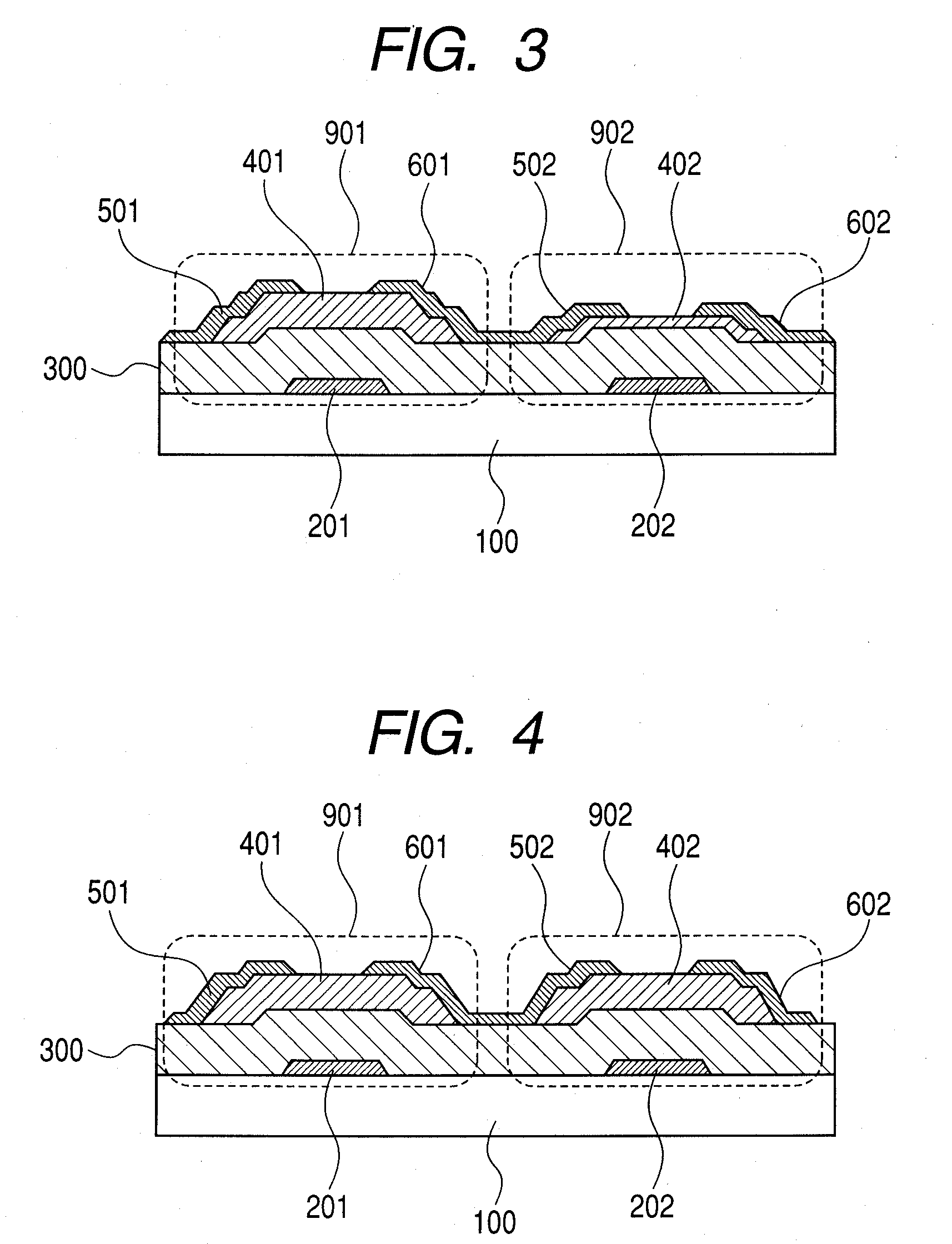
[0048]A part of a cross sectional view of an inverter according to the first embodiment of the present invention is indicated in FIG. 3.
[0049]A first TFT 901 and a second TFT 902 are fabricated on a substrate 100.
[0050]The first TFT 901 includes a first gate electrode 201, an insulator layer 300, a first channel layer 401, a first drain electrode 501 and a first source electrode 601.
[0051]The second TFT 902 includes a second gate electrode 202, the insulator layer 300, a second channel layer 402, a second drain electrode 502 and a second source electrode 602.
[0052]Here, the insulator layer 300 is integrally built into the first TFT 901 and the second TFT 902. However, it may be separately built into the each TFT.
[0053]The first source electrode 601 and the second drain electrode 502 are connected with each other. The first gate electrode 201 is connected with the first source electrode 601 by a wiring (not illustrated).
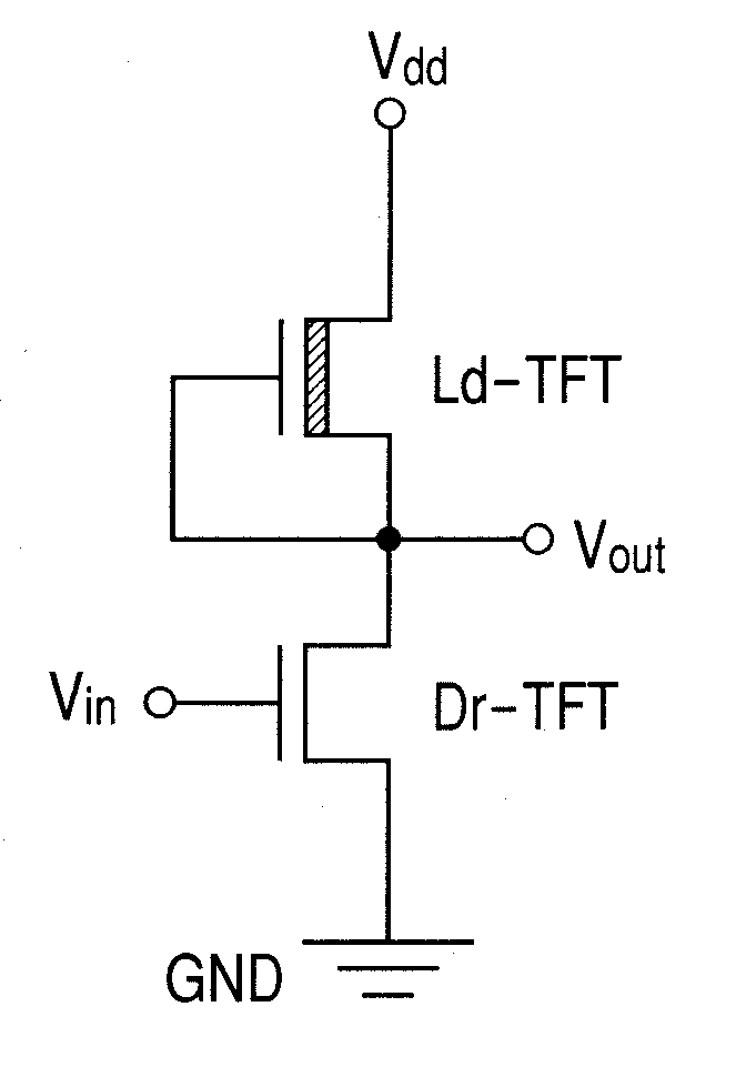
[0054]When the first drain electrode 501 is connected to the pow...
second embodiment
[0059]A part of a cross sectional view of an inverter according to the second embodiment of the present invention is indicated in FIG. 4.
[0060]The first TFT 901 and the second TFT 902 are fabricated on the substrate 100.
[0061]The first TFT 901 includes the first gate electrode 201, the insulator layer 300, the first channel layer 401, the first drain electrode 501 and the first source electrode 601.
[0062]The second TFT 902 includes the second gate electrode 202, the insulator layer 300, the second channel layer 402, the second drain electrode 502 and the second source electrode 602.
[0063]The first source electrode 601 and the second drain electrode 502 are connected with each other. The first gate electrode 201 is connected with the first source electrode 601 by a wiring (not illustrated).
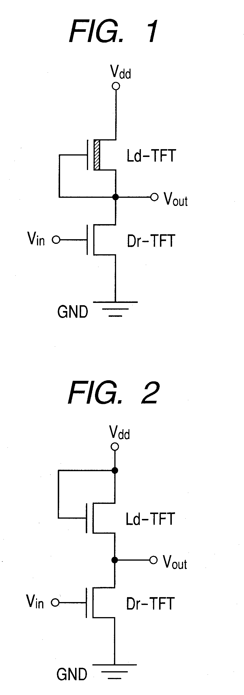
[0064]When the first drain electrode 501 is connected to the power supply voltage Vdd terminal and the second source electrode 602 is connected to the ground, an E / D inverter, where the second gate...
third embodiment
[0084]As indicated in the first embodiment, after fabricating the channel layers having different thickness, the heating process condition of the first channel layer is made to be differed from that of the second channel layer as in a method described in the second embodiment when the thermal process is executed in an arbitrary fabricating process.
[0085]As a result of this method, the first TFT 901 and the second TFT 902 have different values of the voltage Vth.
[0086]In order to operate the E / D inverter according to the present invention effectively, an appropriate range as the difference between threshold voltages of two kinds of transistors will be described. FIG. 5 is a view indicating a result of comparing the oscillation characteristic of a 31-stage ring oscillator based on the saturated load E / E inverters with the oscillation characteristic of a 31-stage ring oscillator based on the E / D inverters by a SPICE (Simulation Program with Integrated Circuit Emphasis) simulation metho...
PUM
 Abstract
Description
Claims
Application Information