Nf3/h2 remote plasma process with high etch selectivity of psg/bpsg over thermal oxide and low density surface defects

a technology of nf3/h2 and remote plasma, applied in the direction of electrical equipment, basic electric elements, electric discharge tubes, etc., can solve the problems of increasing the resistance of devices and degrading the properties of devices

Inactive Publication Date: 2010-04-22
APPLIED MATERIALS INC
View PDF58 Cites 260 Cited by
  • Summary
  • Abstract
  • Description
  • Claims
  • Application Information

AI Technical Summary

Benefits of technology

[0008]Embodiments of the invention provide a method for treating a semiconductor substrate having doped regions and undoped regions, comprising disposing the semiconductor substrate in a processing chamber, providing a reactive gas mixture comprising hydrogen radicals and fluorine radicals to the processing chamber, exposing the semiconductor substrate to the reactive gas mixture, and etching the doped regions of the semiconductor substrate faster than the undoped regions in a carbon-free dry etch process.

Problems solved by technology

The presence of carbon in undesired circumstances can degrade the properties of devices, such as increasing their resistance or changing their dielectric properties.

Method used


Image

  • Nf3/h2 remote plasma process with high etch selectivity of psg/bpsg over thermal oxide and low density surface defects
  • Nf3/h2 remote plasma process with high etch selectivity of psg/bpsg over thermal oxide and low density surface defects
  • Nf3/h2 remote plasma process with high etch selectivity of psg/bpsg over thermal oxide and low density surface defects

Examples


Embodiment Construction

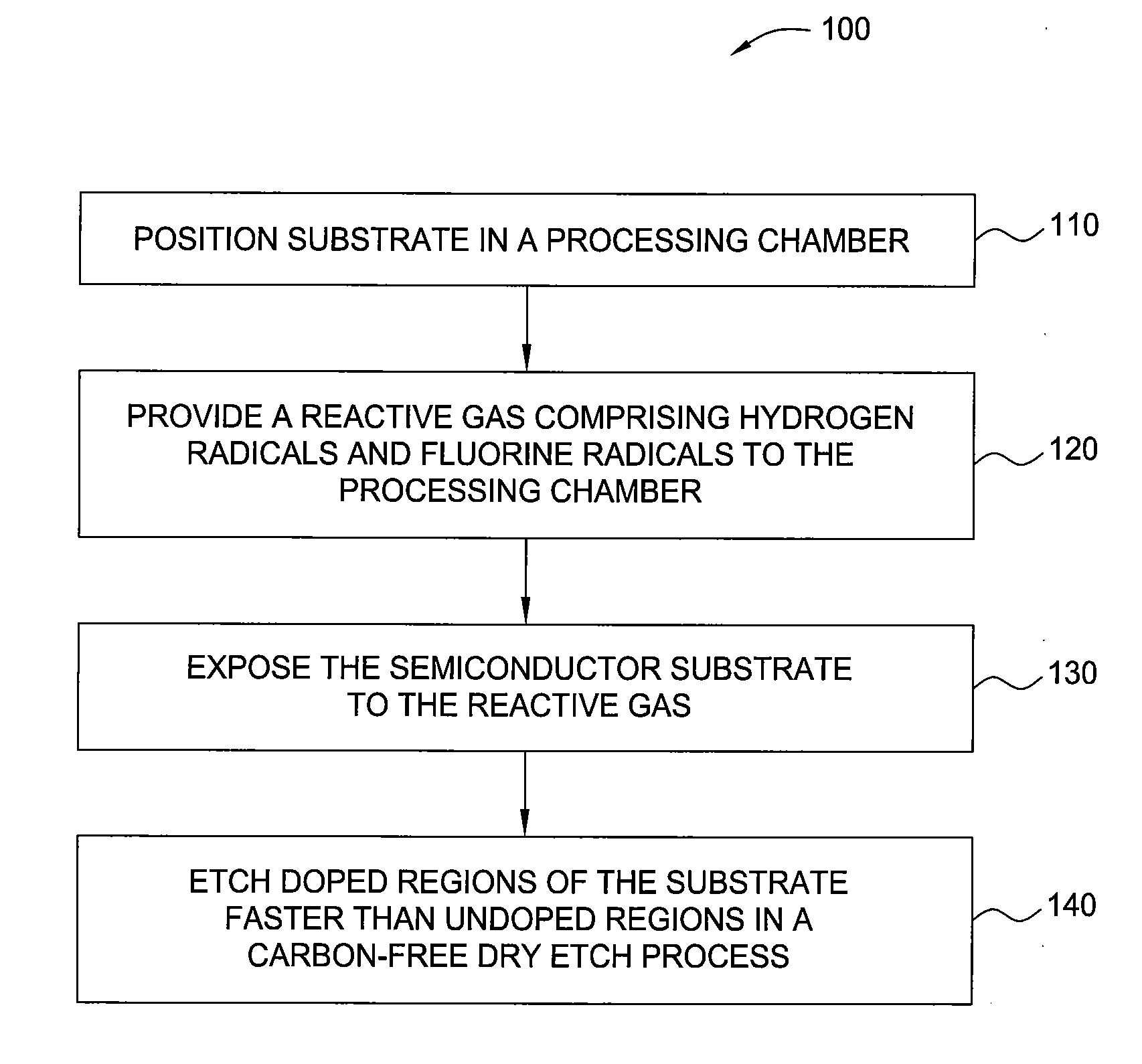
[0017]Embodiments of the invention generally provide methods and apparatus for selectively etching semiconductor substrates having doped and undoped silicate regions. In one aspect, a method for selectively etching such substrates comprises disposing the semiconductor substrate in a processing chamber, providing a reactive gas mixture comprising hydrogen radicals and fluorine radicals to the processing chamber, exposing the semiconductor substrate to the reactive gas mixture, and etching the doped regions of the semiconductor substrate faster than the undoped regions. The semiconductor substrate may have doped and undoped silicate regions, or may have only a doped surface or an undoped surface to be etched. The doped regions or surface will generally be doped with boron or phosphorus atoms or ions, and may be formed by implanting dopants into a semiconductor surface or by deposition with in-situ doping, such as by an epitaxial deposition process.

[0018]FIG. 1 is a flow diagram summar...


PUM


Abstract

A method and apparatus for selectively etching doped semiconductor oxides faster than undoped oxides. The method comprises applying dissociative energy to a mixture of nitrogen trifluoride and hydrogen gas remotely, flowing the activated gas toward a processing chamber to allow time for charged species to be extinguished, and applying the activated gas to the substrate. Reducing the ratio of hydrogen to nitrogen trifluoride increases etch selectivity. A similar process may be used to smooth surface defects in a silicon surface.

Description

BACKGROUND OF THE INVENTION[0001]1. Field of the Invention[0002]Embodiments of the invention relate to methods of treating semiconductor substrates. More particularly, embodiments of the invention provide methods of selectively etching layers on semiconductor substrates.[0003]2. Description of the Related Art[0004]Doped silicates are widely used in the semiconductor industry for many applications. They may be used as interlayer insulators in some cases, or as semiconductive regions for CMOS devices. In some cases they are formed by depositing a doped layer on a substrate, while in other cases they may be formed by implanting dopants into a substantially pure semiconductor layer. In many instances, doped silicates are used alongside pure silicates to provide a chemical difference by which treatment of the different materials may be differentiated.[0005]In some instances, a doped silicate layer may be used as an etch-stop layer for an undoped silicate layer. In those cases, an etching...

Claims


Application Information

Patent Timeline
Patent Type & Authority Applications(United States)
IPC IPC(8): H01L21/34H01L21/465H01L21/428
CPCH01J37/32357H01J37/32422H01L21/67109H01L21/67069H01L21/31116
Inventor KAO, CHIEN-TEHLU, XINLIANGYANG, HAICHUNGE, ZHENBINOR, DAVID T.CHANG, MEI
Owner APPLIED MATERIALS INC
Why Eureka
Try Eureka