Semiconductor device and manufacturing method thereof

a semiconductor amplifier and manufacturing method technology, applied in the direction of transistors, printed circuit aspects, basic electric elements, etc., can solve the problems of reducing the size of the electronic components mounted on the wiring board, not being able being inefficient in trying to achieve the size reduction of the rf power module, etc., to achieve the reduction of the mounting area of the semiconductor amplifier element chip, the effect of reducing the size of the rf power

Active Publication Date: 2010-05-06
MURATA MFG CO LTD
View PDF4 Cites 85 Cited by
  • Summary
  • Abstract
  • Description
  • Claims
  • Application Information

AI Technical Summary

Benefits of technology

[0011]In such circumstances, the structure of an RF power module in which a semiconductor amplifier element chip is flip-chip mounted on a wiring board has been developed. In this case, since the mounting area of the semiconductor amplifier element chip is reduced compared with the case where a semiconductor amplifier element chip is face-up bonded on a wiring board and electrodes of the semiconductor amplifier element chip and terminals of the wiring board are wire-bonded, the planar dimensions of the wiring board can be reduced, so that the size reduction of the RF power module can be achieved.
[0012]However, the case where a semiconductor amplifier element chip is flip-chip mounted on a wiring board is disadvantageous in the heat dissipation properties compared with the case where a semiconductor amplifier element chip is face-up bonded on a wiring board. This is because an entire rear surface of a semiconductor amplifier element chip is bonded to a wiring board when the semiconductor amplifier element chip is face-up bonded and the heat can be dissipated from the entire rear surface of the semiconductor amplifier element chip to the wiring board side, whereas the heat generated in the semiconductor amplifier element chip is dissipated to the wiring board side via bump electrodes of the semiconductor amplifier element chip when the semiconductor amplifier element chip is flip-chip mounted. When an LDMOSFET element making up a power amplifier circuit is formed in a semiconductor amplifier element chip, the considerably large amount of heat is generated from the LDMOSFET element. Therefore, it is extremely important to improve the heat dissipation properties when a semiconductor amplifier element chip is flip-chip mounted on a wiring board, thereby improving the performance and reliability of the RF power module.
[0013]An object of the present invention is to provide a technique capable of reducing the size of a semiconductor device.
[0014]Also, another object of the present invention is to provide a technique capable of improving the properties of a semiconductor device, in particular, heat dissipation properties.

Problems solved by technology

However, there is a limitation on the size reduction of the electronic components mounted on the wiring board, and it is not efficient to try to achieve the size reduction of the RF power module only by the size reduction of the electronic components.
However, the case where a semiconductor amplifier element chip is flip-chip mounted on a wiring board is disadvantageous in the heat dissipation properties compared with the case where a semiconductor amplifier element chip is face-up bonded on a wiring board.

Method used


Image

  • Semiconductor device and manufacturing method thereof
  • Semiconductor device and manufacturing method thereof
  • Semiconductor device and manufacturing method thereof

Examples


first embodiment

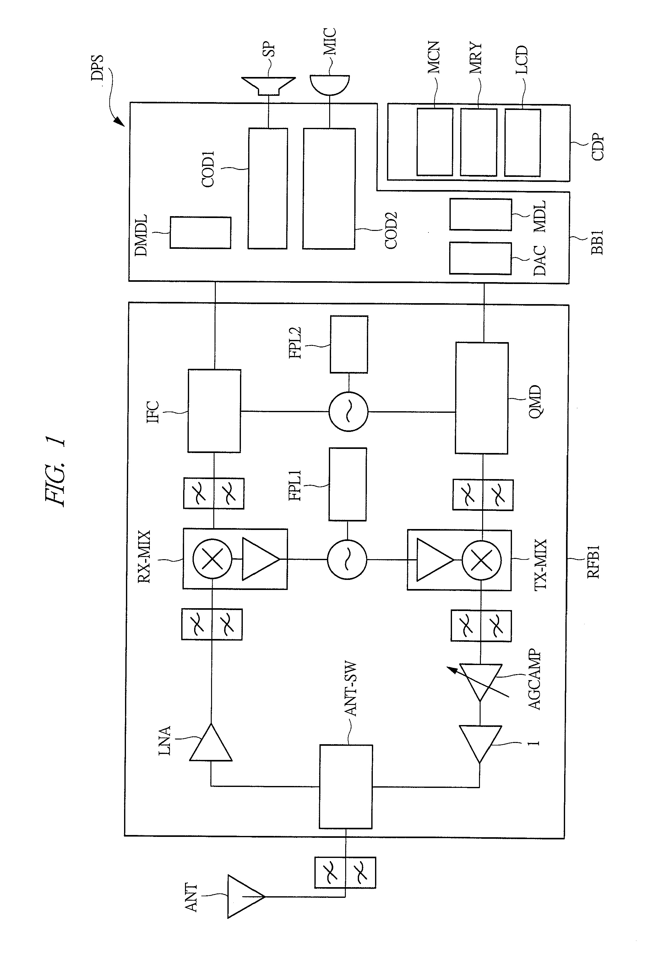
[0096]The present embodiment is a power amplifier module (semiconductor device) such as an RF (Radio Frequency) power module used (mounted) in a digital mobile phone (mobile communication system) transmitting information through a network of, for example, the GSM system and is a semiconductor chip (semiconductor device) used (mounted) in the power amplifier module.

[0097]Here, the GSM (Global System for Mobile Communication) is one of wireless communication systems or standards used for the digital mobile phone. There are three frequency bands defined for GSM. Of these, a 900 MHz band (824-915 MHz) is called GSM900 or simply GSM, a 1800 MHz band (1710-1910 MHz) is called GSM1800, DCS1800 (Digital Cellular System 1800) or PCN, and a 1900 MHz band is called GSM1900, DCS1900 or PCS (Personal Communication Services). GSM1900 is mainly used in North America. In addition, GSM850 which operates in a 850 MHz band is sometimes used in North America. A power amplifier module of the present emb...

second embodiment

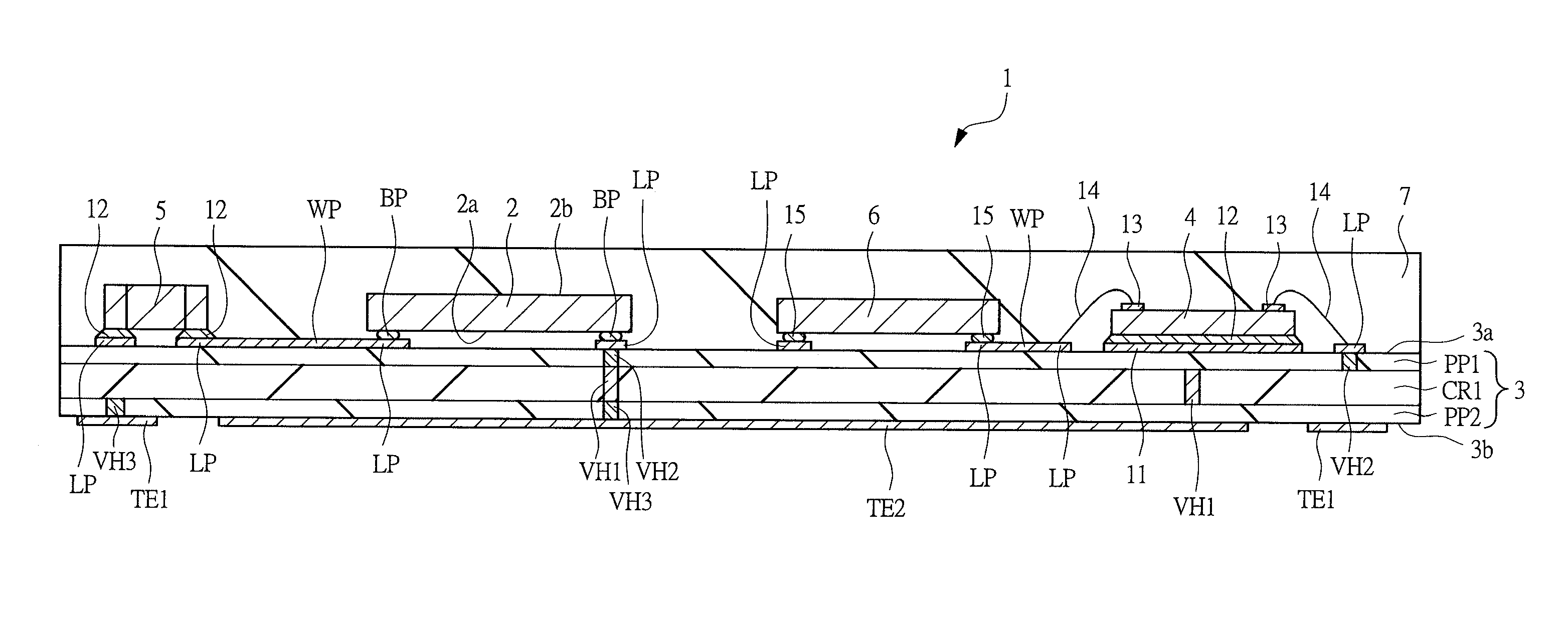
[0372]FIG. 40 is a plan view of the principal part of the semiconductor chip 2 of the present embodiment, and it corresponds to FIG. 28 of the first embodiment described above. Similarly to FIG. 28, the planar layout of the source bump electrode BPS, the drain bump electrode BPD and the gate bump electrode BPG is shown by solid lines in FIG. 40. Also, in FIG. 40, the source conductor layer CNDS, the drain conductor layer CNDD and the gate conductor layer CNDG are shown by broken lines, the source pad M3S, the drain pad M3D and the gate pad M3G are shown by two-dot chain lines, and the LDMOSFET formation region REG1 is shown by broken lines so as to make the positional relation easily understood. FIG. 41 is a plan view of the principal part of the semiconductor chip 2 of the present embodiment showing the same region as FIG. 40, and it corresponds to FIG. 35 described above. In FIG. 41, the layout of the source bump electrode BPS, the drain bump electrode BPD and the gate bump electr...

third embodiment

[0403]The present embodiment relates to a semiconductor device and a manufacturing technique thereof, and more particular to a technique effectively applied to a semiconductor device including a heterojunction bipolar transistor (HBT) and a manufacturing technique thereof.

[0404]For example, some semiconductor elements use a III-V group compound semiconductor such as gallium arsenide (GaAs). The compound semiconductor is characterized in that it has higher mobility than silicon (Si) and semi-insulating crystal can be obtained. Also, the compound semiconductor can form a mixed crystal, and the heterojunction can be formed.

[0405]The semiconductor element using the heterojunction includes the heterojunction bipolar transistor (hereinafter, HBT). This HBT is a bipolar transistor using gallium arsenide as a base layer and using indium gallium phosphide (InGaP) or aluminum gallium phosphide (AlGaAs) as an emitter layer. More specifically, HBT is a bipolar transistor in which the heterojunc...


PUM


Abstract

In a semiconductor chip in which LDMOSFET elements for power amplifier circuits used for a power amplifier module are formed, a source bump electrode is disposed on an LDMOSFET formation region in which a plurality of source regions, a plurality of drain regions and a plurality of gate electrodes for the LDMOSFET elements are formed. The source bump electrode is formed on a source pad mainly made of aluminum via a source conductor layer which is thicker than the source pad and mainly made of copper. No resin film is interposed between the source bump electrode and the source conductor layer.

Description

CROSS-REFERENCE TO RELATED APPLICATION[0001]The present application claims priority from Japanese Patent Application No. JP 2008-283810 filed on Nov. 5, 2008, Japanese Patent Application No. JP 2009-97248 filed on Apr. 13, 2009, and Japanese Patent Application No. JP 2009-198360 filed on Aug. 28, 2009, the contents of which are hereby incorporated by reference into this application.TECHNICAL FIELD OF THE INVENTION[0002]The present invention relates to a semiconductor device and a manufacturing method thereof, and more particularly to a technique effectively applied to a power amplifier module mounted on a mobile communication system, a semiconductor device used therein and a manufacturing method thereof.BACKGROUND OF THE INVENTION[0003]In recent years, mobile communication systems represented by such communication systems as GSM system, PCS system, PDC system and CDMA system (so-called mobile phone) have spread worldwide.[0004]In general, the mobile communication system of this type...

Claims


Application Information

Patent Timeline
Patent Type & Authority Applications(United States)
IPC IPC(8): H01L27/082H01L27/088H01L21/8222H01L29/78
CPCH01L21/823425H01L21/823475H01L23/66H01L24/11H01L24/12H01L24/16H01L24/17H01L24/28H01L24/29H01L24/32H01L24/48H01L25/16H01L27/088H01L29/04H01L29/0692H01L29/0847H01L29/1087H01L29/41758H01L29/66659H01L29/7371H01L29/7835H01L2223/6644H01L2223/6677H01L2224/13099H01L2224/16225H01L2224/32225H01L2224/48091H01L2224/48227H01L2224/49171H01L2224/73265H01L2924/01004H01L2924/01005H01L2924/01013H01L2924/01015H01L2924/01022H01L2924/01027H01L2924/01029H01L2924/0103H01L2924/01042H01L2924/01046H01L2924/01047H01L2924/01049H01L2924/0105H01L2924/01074H01L2924/01078H01L2924/01079H01L2924/01082H01L2924/014H01L2924/04941H01L2924/10329H01L2924/10336H01L2924/13091H01L2924/14H01L2924/19041H01L2924/19042H01L2924/19043H01L2924/19105H01L2924/30105H01L2924/3011H05K1/0206H05K2201/09481H05K2201/096H05K2201/10674H01L2924/01024H01L24/49H01L2924/01006H01L2924/01023H01L2924/01033H01L2924/0132H01L24/73H01L2924/0133H01L2224/29111H01L2224/291H01L2924/1517H01L2924/12041H01L2924/13064H01L2224/16235H01L2224/05553H01L2224/0401H01L2924/1306H01L2924/181H01L2224/1134H01L2224/13144H01L2924/1305H01L2924/30111H01L2924/00014H01L2924/10161H01L2224/05171H01L2224/05644H01L2224/05666H01L29/0878H01L2224/05164H01L2224/05147H01L2224/05155H01L2924/00H01L2924/01028H01L2924/01032H01L2924/01083H01L2924/00012H01L2224/45099H01L2224/45015H01L2924/207H01L24/13H01L24/05H01L24/03H01L2224/02166H01L23/4824H01L2924/013
Inventor NAKAJIMA, SHIZUKINAGAI, HIROYUKISHIRAI, YUJINAKEJIMA, HIROKAZUKUSANO, CHUSHIROHASEGAWA, YUYORITA, CHIKOOSONE, YASUO
Owner MURATA MFG CO LTD
Why Eureka
Try Eureka