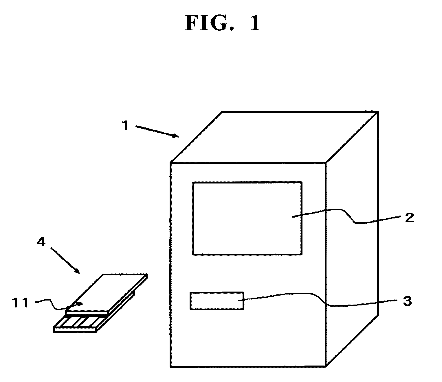
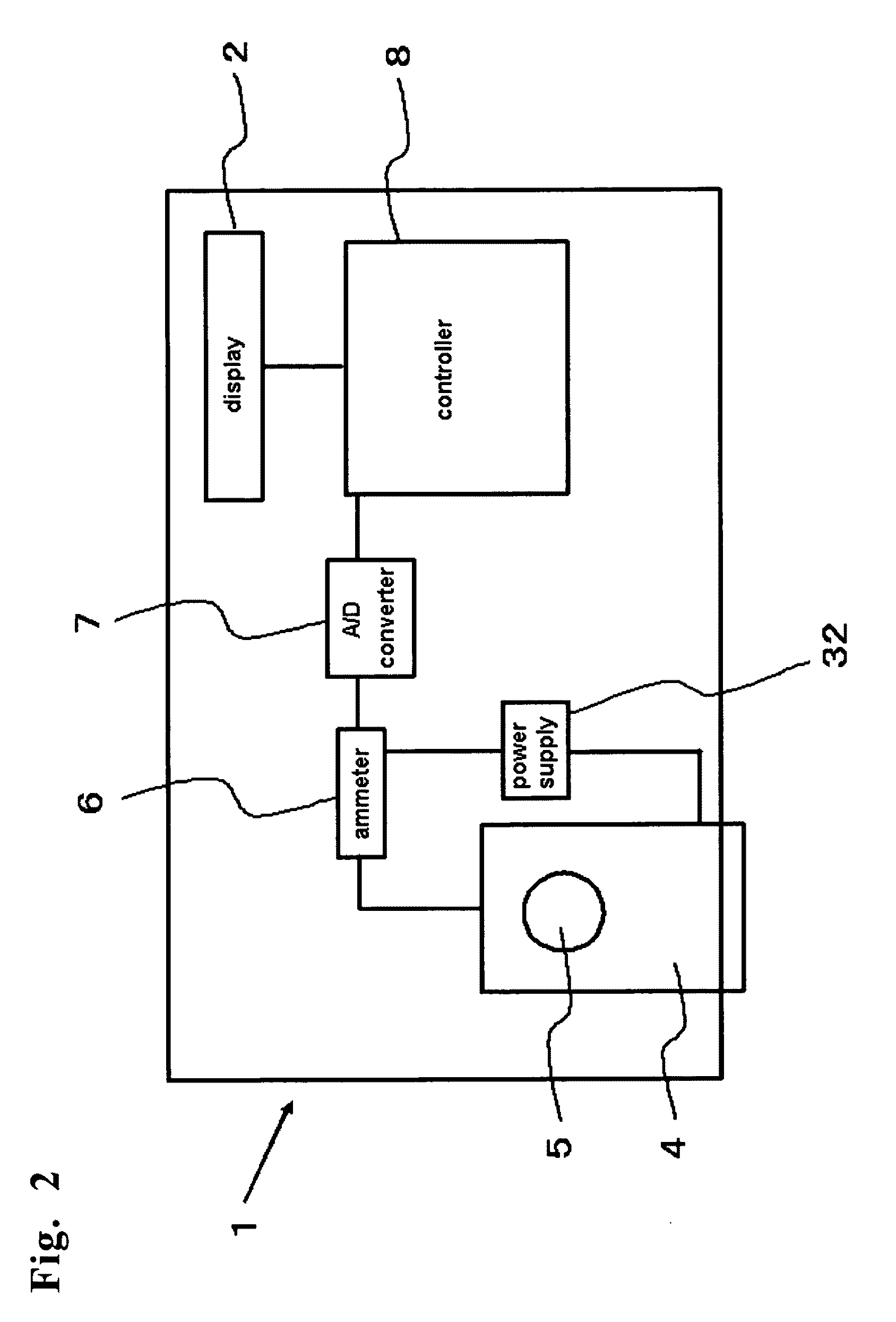
Test chip, detection apparatus, and method for detecting analyte
a detection apparatus and analyte technology, applied in the field of test chips, can solve the problems of reducing the detection efficiency, and low sensitivity of the detection of analyte, and achieve the effects of improving the detection efficiency, reducing the cost, and improving the detection efficiency
- Summary
- Abstract
- Description
- Claims
- Application Information
AI Technical Summary
Problems solved by technology
Method used
Image

Examples
example 1
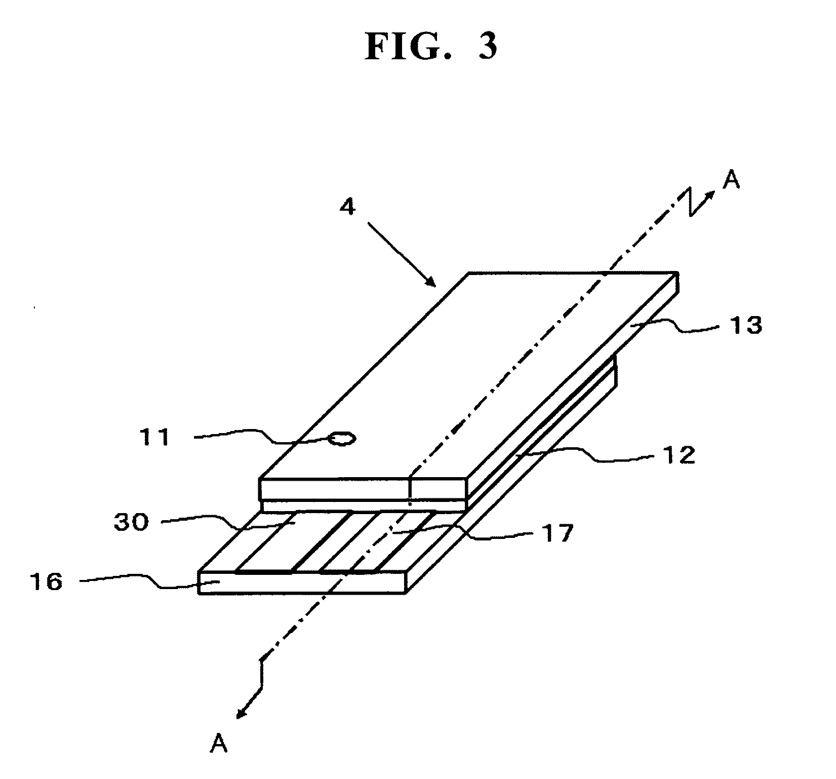
Examination of the Presence or Absence of Metal Layer on Semiconductor Electrode
(Preparation of Semiconductor Electrode Part)
[0076]Indium tin oxide (ITO) and antimony-doped tin oxide (ATO) were formed with a thickness of 100 nm as a conductive layer by sputtering on a substrate made of silicon dioxide (SiO2). On this conductive layer, titanium oxide (TiO2) was formed as a semiconductor layer of 10 nm in thickness by sputtering, and a gold thin film was formed as a metal layer of 10 nm in thickness thereon. By using a semiconductor layer containing titanium or chrome, the adhesion between the gold thin film and the semiconductor layer is improved. The member containing the conductive layer, the semiconductor layer and the metal layer is referred to the semiconductor electrode part. A semiconductor electrode lead for connection to an ammeter is connected to the semiconductor electrode part.
(Preparation of Counter Electrode Part)
[0077]A platinum thin layer formed with a thickness of 20...
example 2
Detection by Current Measurement of Analyte Modified with Modulator
(Preparation of Semiconductor Electrode Part)
[0089]Prepared in the same manner as in Example 1.
(Preparation of Counter Electrode)
[0090]Prepared in the same manner as in Example 1.
(Immobilization of Probe)
[0091]Performed in the same manner as in Example 1.
(Preparation of Analyte)
[0092]An analyte (analyte A) having a modulator bound to a DNA containing a nucleotide sequence complementary to the probe and an analyte (analyte B) having a modifier bound to a DNA not containing a nucleotide sequence complementary to the probe are prepared as analytes.
[0093]The modulator is a sensitizing dye Pulsar 650 (manufactured by Bio Search Technologies Japan). This sensitizing dye is a ruthenium complex and is bound to the DNA via a peptide bond.
(Trap of Analyte with Probe)
[0094]The analyte A or B is subjected to hybridization reaction with the probe on the metal layer. First, silicon rubber (thickness 0.2 mm) is arranged as a partit...
example 3
Effect of the Semiconductor Electrode Using Modulator Excited with Long Wavelength
(Preparation of Semiconductor Electrode Part)
[0106]Indium tin oxide (ITO) was formed with a thickness of 100 nm as a conductive layer by sputtering on a substrate made of silicon dioxide (SiO2). On this conductive layer, indium oxide (In2O3) was formed as a semiconductor layer of 10 nm in thickness by sputtering, and a gold thin film was formed as a metal layer of 10 nm in thickness thereon. It was calcinated (150° C.) in an oxygen atmosphere, thereby improving the adhesion between the gold thin film and the semiconductor layer. The member containing the conductive layer, the semiconductor layer and the metal layer is referred to the semiconductor electrode part. A semiconductor electrode lead for connection to the ammeter is connected to the semiconductor electrode part.
(Preparation of Counter Electrode Part)
[0107]Prepared in the same manner as in Example 1.
(Immobilization of Probe Substance)
[0108]A p...
PUM
| Property | Measurement | Unit |
|---|---|---|
| Current | aaaaa | aaaaa |
| Electrical conductor | aaaaa | aaaaa |
| Wavelength | aaaaa | aaaaa |
Abstract
Description
Claims
Application Information
 - R&D
- Intellectual Property
- Life Sciences
- Materials
- Tech Scout
- Unparalleled Data Quality
- Higher Quality Content
- 60% Fewer Hallucinations
Browse by: Latest US Patents, China's latest patents, Technical Efficacy Thesaurus, Application Domain, Technology Topic, Popular Technical Reports.
© 2025 PatSnap. All rights reserved.Legal|Privacy policy|Modern Slavery Act Transparency Statement|Sitemap|About US| Contact US: help@patsnap.com