Methods of manufacturing trench isolated drain extended mos (DEMOS) transistors and integrated circuits therefrom

Active Publication Date: 2010-05-13
TEXAS INSTR INC
View PDF2 Cites 34 Cited by
  • Summary
  • Abstract
  • Description
  • Claims
  • Application Information

AI Technical Summary

Benefits of technology

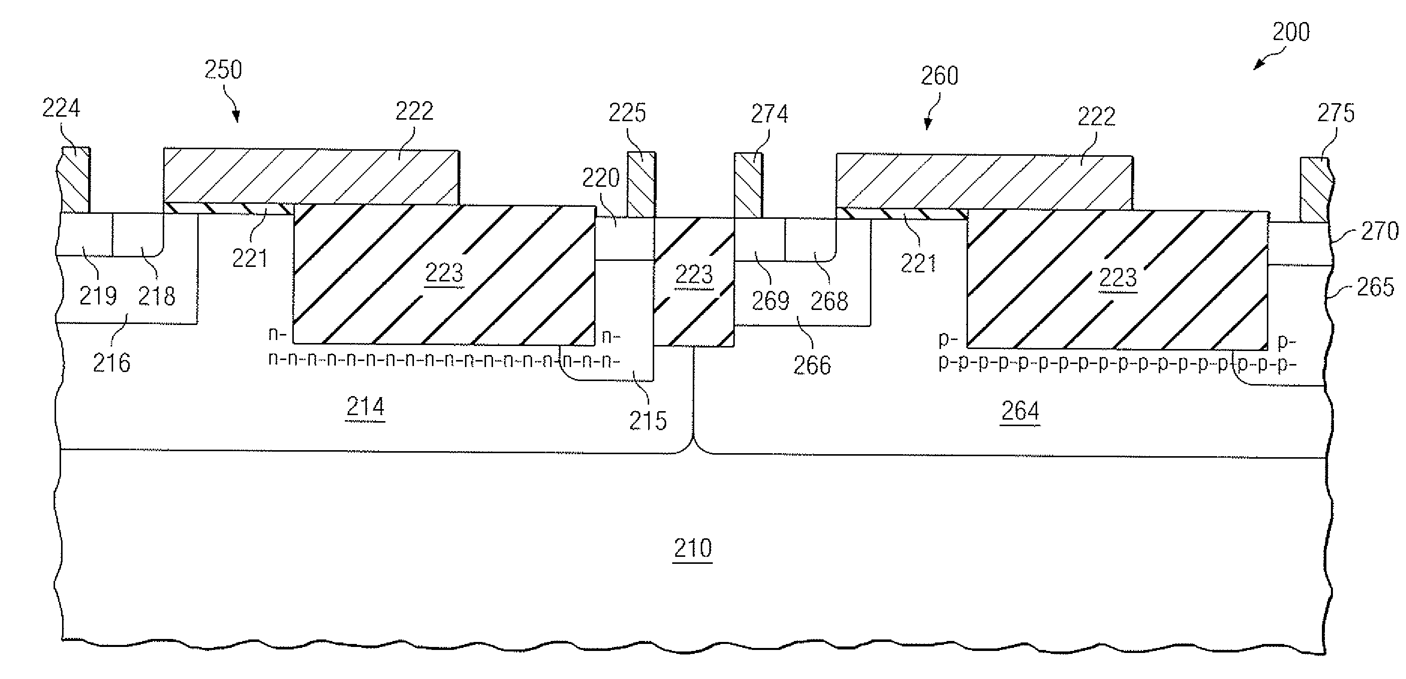
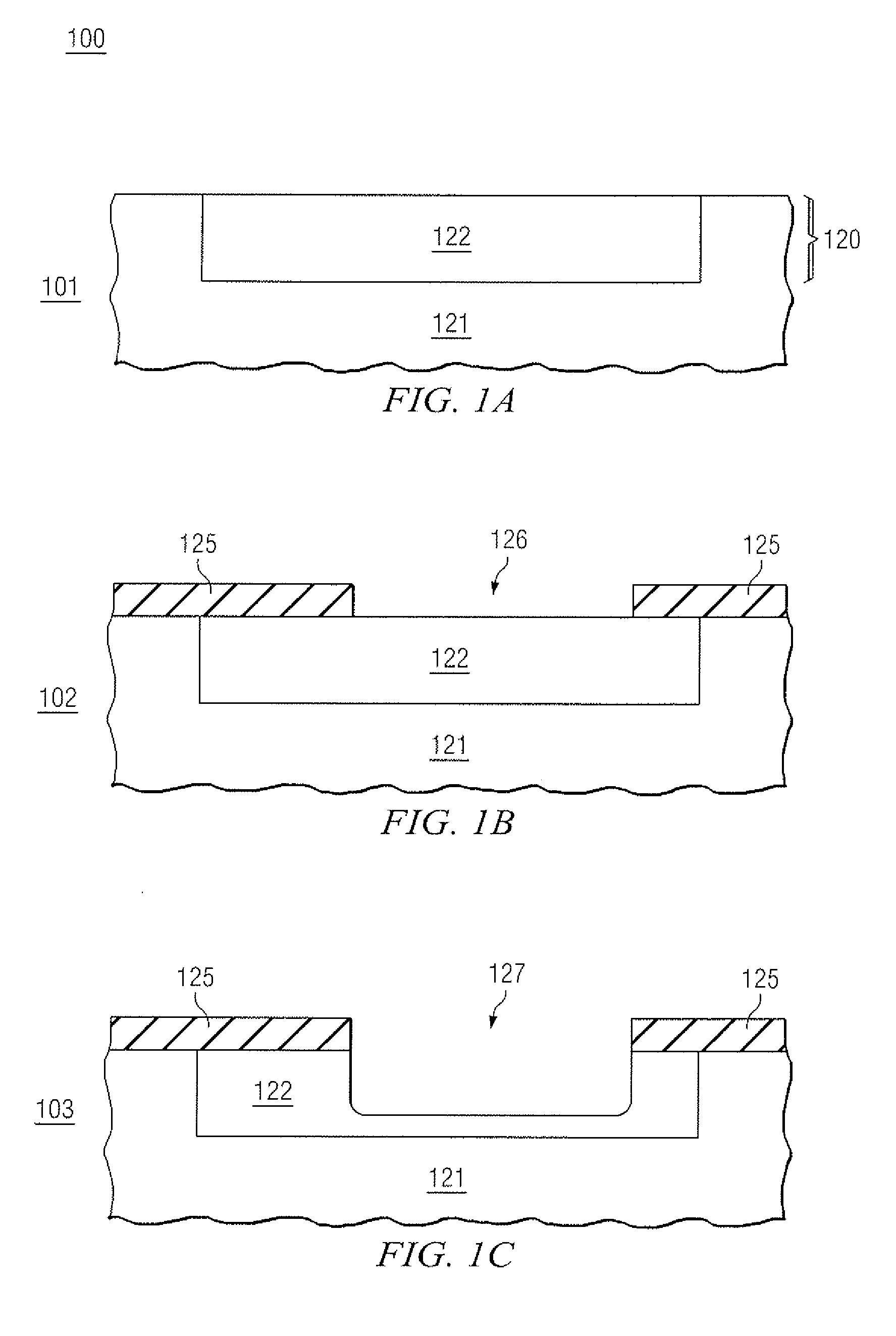
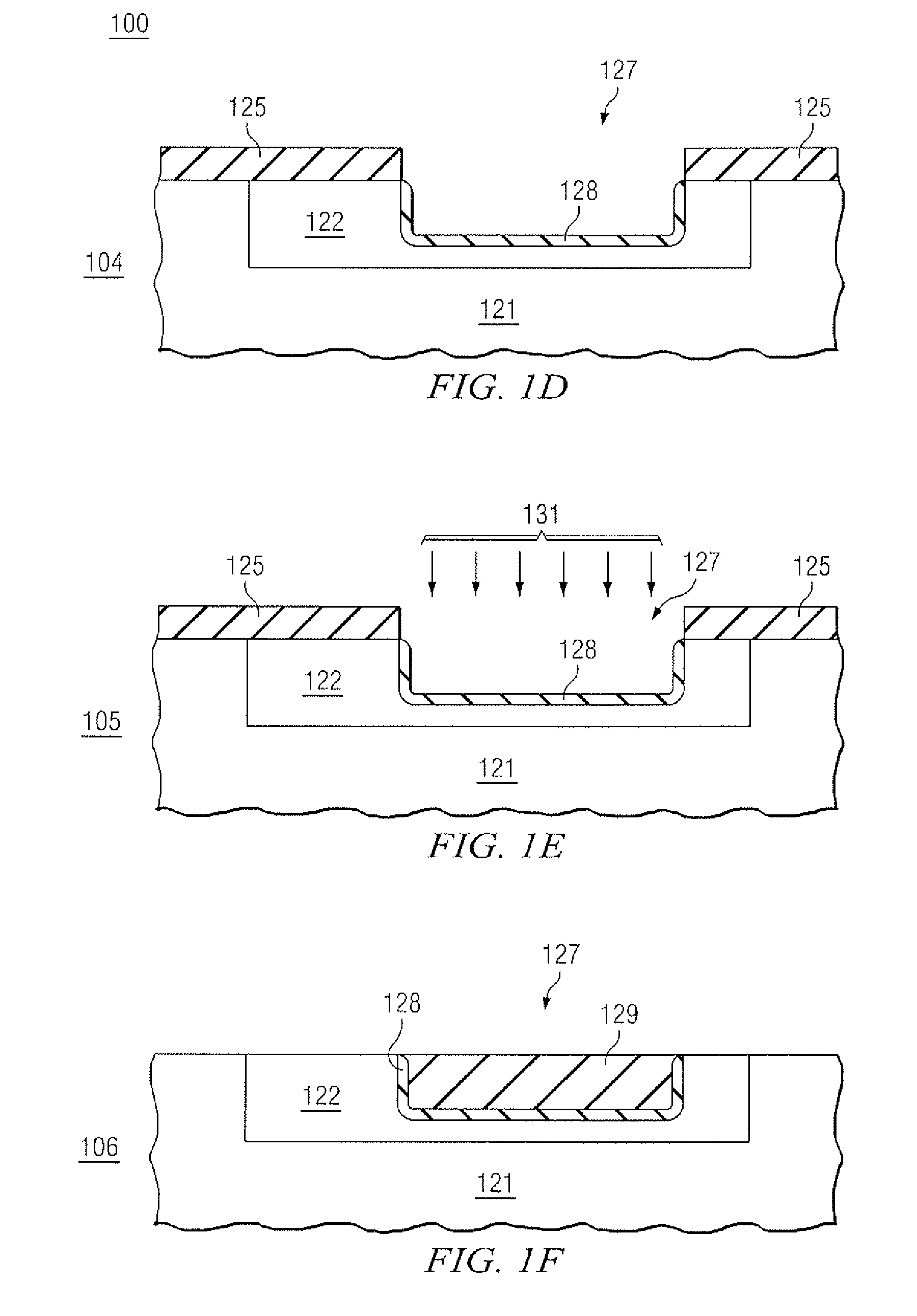
[0007]Embodiments of the present invention generally include an additional n-type implant through the trench but before the trench is filled. This implant is hereafter generally referred to as an Rdson reduction implant, due to its significant reduction of Rdson. The Rdson reduction implant boosts the oxide/Si interface n-type concentration in the n-drift region as compared to the n-type dopant concentration at the semiconductor surface under the gate, such as by a factor of at least 3 (three), and generally by a factor of at least 5 (five), thus lowering Rdson. The Rdson reduction implant occurring after trench etch helps reduce dopant sensitivity in the n-drift region due to trench isolation (e.g. STI) depth variation. Moreover, Rdson reduction implants according to embodiments of the inve

Problems solved by technology

Since the field oxide thickness is usually limited by technological constraints, higher breakdown voltages typically require more lightly doped layers.
However, for trench isolation based processes (e.g. shallow trench isolation (STI)), n-type dopant pileup is not available to increase the n-type doping along the field oxide/Si interface n-drift region to lessen the tradeoff between BVdss, Rdson and BVon.
Moreover, the Present Inv

Method used


Image

  • Methods of manufacturing trench isolated drain extended mos (DEMOS) transistors and integrated circuits therefrom
  • Methods of manufacturing trench isolated drain extended mos (DEMOS) transistors and integrated circuits therefrom
  • Methods of manufacturing trench isolated drain extended mos (DEMOS) transistors and integrated circuits therefrom

Examples


examples

[0027]The following non-limiting Examples serve to illustrate selected embodiments of the invention. It will be appreciated that variations in proportions and alternatives in elements of the components shown will be apparent to those skilled in the art and are within the scope of embodiments of the present invention.

[0028]FIG. 3 is a graph of current vs. drain to source voltage for a control DENMOS device (no Rdson reduction implant) and a DENMOS device according to an embodiment of the invention having an Rdson reduction implant. FIG. 3 also includes a data table that provides values for Rdson, BVdss and BVon data from the graph for the control DENMOS device and the DENMOS device according to an embodiment of the invention. The Rdson reduction implant comprised an As dose of 5×1011 cm2 at 160 keV. The liner oxide through which the implant was performed was around 150 Angstroms. Rdson, BVdss and BVon can all be seen to be significantly improved for the DENMOS device according to an ...


PUM


Abstract

A method of fabricating an integrated circuit (IC) including at least one drain extended MOS (DEMOS) transistor and ICs therefrom includes providing a substrate having a semiconductor surface, the semiconductor surface including at least a first surface region that provides a first dopant type. A patterned masking layer is formed on the first surface region, wherein at least one aperture in the masking layer is defined. The first surface region is etched to form at least one trench region corresponding to a position of the aperture. A dopant of a first dopant type is implanted to raise a concentration of the first dopant type in a first dopant type drift region located below the trench region. After the implanting, the trench region is filled with a dielectric fill material. A body region is then formed having a second dopant type in a portion of the first surface region. A gate dielectric is then formed over a surface of the body region and the first surface region. A patterned gate electrode layer is formed over the gate dielectric, a source region in the body region and a drain region in the first surface region on a side of the trench region opposite to the source are formed, and fabrication of the IC is completed.

Description

FIELD OF THE INVENTION[0001]Embodiments of the present invention relate to methods of manufacturing integrated circuits (ICs) that include high voltage devices, and in particular to methods of manufacturing trench isolated drain extended MOS (DEMOS) transistors and ICs therefrom.BACKGROUND[0002]Power semiconductor products are often fabricated using N or P channel drain-extended metal-oxide-semiconductor (DENMOS and DEPMOS, respectively) transistor devices, such as lateral diffused MOS (LDMOS) devices, for high power switching applications. DEMOS devices advantageously combine short-channel operation with high current handling capabilities, relatively low drain-source on-state resistance (Rdson), and the ability to withstand high blocking voltages without suffering voltage breakdown failure. Breakdown voltage is typically measured as drain-to-source breakdown voltage with the gate and source shorted together (BVdss).[0003]DEMOS structures generally include thick local oxidation (LOC...

Claims


Application Information

Patent Timeline
IPC IPC(8): H01L27/06H01L21/336
CPCH01L21/823814H01L21/823892H01L29/0653H01L29/7816H01L29/42368H01L29/66681H01L29/0878
Inventor PENDHARKAR, SAMEER PRAKASHHU, BINGHUA NA
Owner TEXAS INSTR INC
Why Eureka
Try Eureka