Avalanche photodiode

a photodiode and avalanche technology, applied in the field of ultrafast avalanche photodiodes, can solve the problems of increasing the dark current around the junction periphery of the device, affecting the production cost of the technique, and affecting the production efficiency of the technique, so as to achieve low dark current and high control

Active Publication Date: 2010-07-01
NTT ELECTORNICS CORP +1
View PDF0 Cites 13 Cited by
  • Summary
  • Abstract
  • Description
  • Claims
  • Application Information

AI Technical Summary

Benefits of technology

[0018]According to the present invention, it is possible to relax the edge electric field in the peripheral part of the avalanche multiplication region without using a diffusion technique, and therefore possible to produce an electron-injection type APD with low dark current in a highly controlled manner.

Problems solved by technology

As a result, a fundamental problem arises in which dark current is increased around the junction periphery of the device.
However, even the proposed techniques described above have the following problems still remained to be solved.
In the technique proposed in the nonpatent document 1, implanting a mesa structure of a semiconductor by regrowth is generally difficult, since growth behavior varies according to plane index.
The technique also has a disadvantage in terms of production cost.
As described above, although it is expected that the electron-injection type APD demonstrates superior features to those of the conventional hole-injection type APD, there were problems in terms of an increase of dark current and securing the device life time.
A structure has also been proposed in which a mesa is buried in APD by use of semiconductor; however, the problems in difficulty of the production technique and production cost still remain to be solved.

Method used


Image

  • Avalanche photodiode
  • Avalanche photodiode
  • Avalanche photodiode

Examples


first embodiment

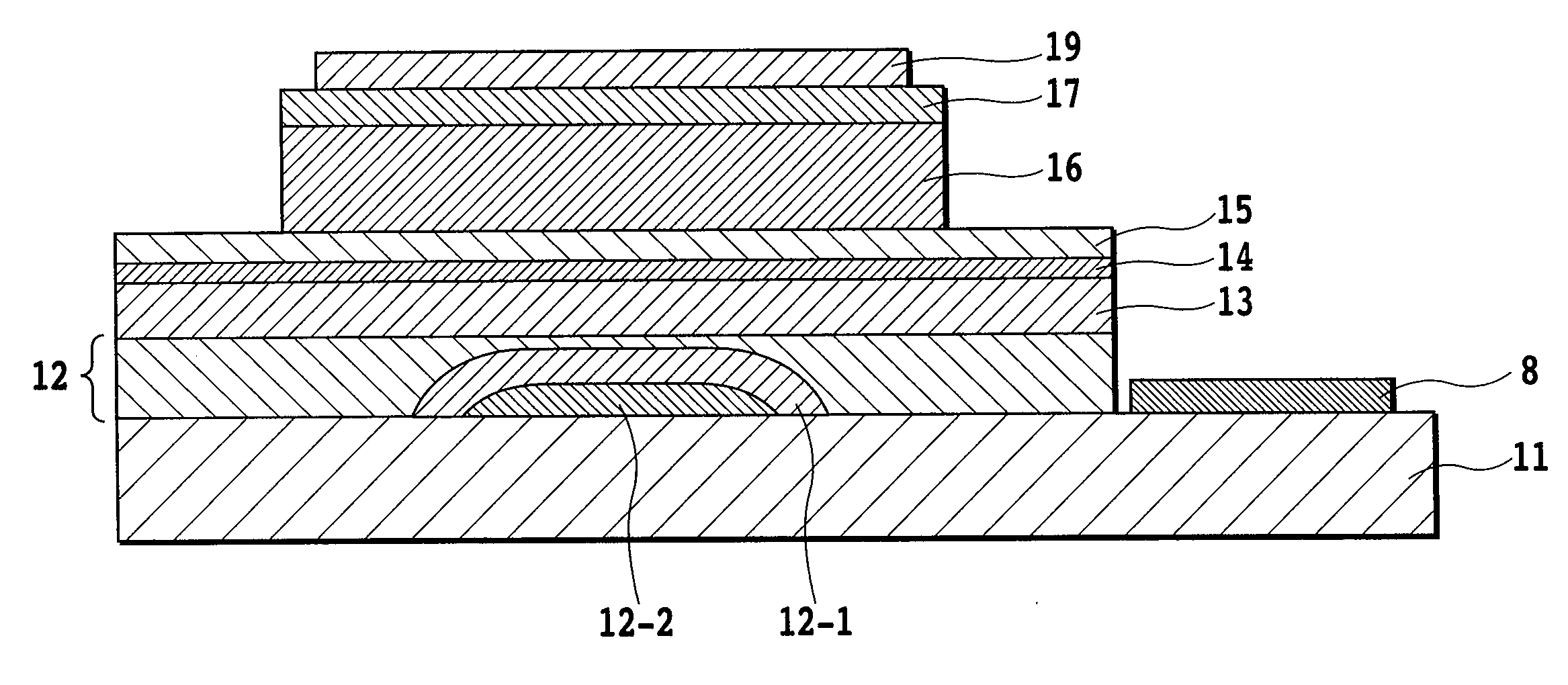
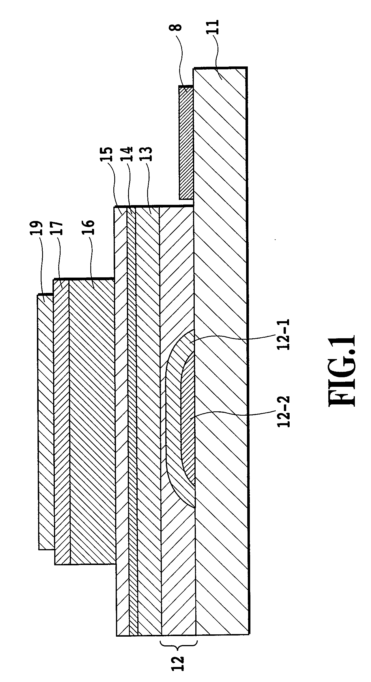
[0024]FIG. 1 is a structural drawing of an APD in accordance with a first embodiment of the present invention. On an n-type InP electrode layer 11, an InP buffer layer 12, an InP avalanche multiplication layer 13, an InP electric field control layer 14, and an InGaAsP bandgap graded layer 15 are formed in order. Furthermore, on the InGaAsP bandgap graded layer 15, a p-type

[0025]InGaAs optical absorption layer 16 in a mesa structure, a p-type InGaAsP electrode layer 17, and a metal electrode 18 are provided. On the n-type InP electrode layer 11, a metal electrode 19 is also provided.

[0026]In addition, n-type InP doping regions 12-1 and 12-2 are formed locally within the InP buffer layer 12. The n-type InP doping region 12-2 is included within the n-type InP doping region 12-1. Furthermore, the n-type InP doping regions 12-1 and 12-2 have different doping concentrations. The structure and the fabrication method will be explained in detail in the later section. As will hereinafter be e...

second embodiment

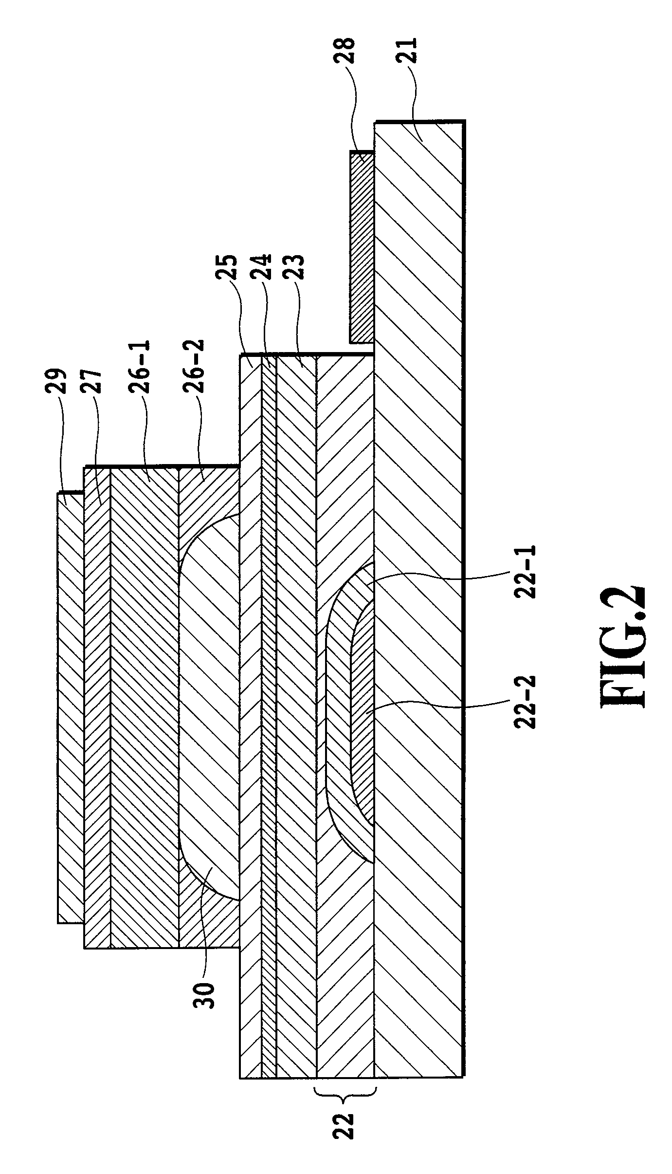
[0035]FIG. 2 is a structural drawing of an APD in accordance with a second embodiment of the present invention. On an n-type InP electrode layer 21, an InP buffer layer 22, an InP avalanche multiplication layer 23, an InP electric field control layer 24, and an InGaAsP bandgap graded layer 25 are sequentially formed. Furthermore, on the InGaAsP bandgap graded layer 25, an optical absorption layer and others which make up a mesa structure are formed. What is characteristic of the present invention is the provision of a second optical absorption layer.

[0036]To be more specific, on the InGaAsP bandgap graded layer 25, a low-concentration second InGaAs optical absorption layer 26-2, which is depleted in an operating state, is firstly formed. On the top of this, as described in the first embodiment, a first p-type InGaAs optical absorption layer 26-1, a p-type InGaAsP electrode layer 27, and a metal electrode 29 are provided. On the top of the n-type InP electrode layer 21, a metal elect...


PUM


Abstract

In an electron-injection type APD, it is necessary to prevent a dark current increase and to secure the life time of the device. It is demanded to improve reliability of the APD with a lower production cost. With the InP buffer layer having an n-type doping region on the inside of a region defined by an optical absorption layer, a predetermined doping profile is achieved by ion implantation. Thus, electric field concentration in the avalanche multiplication layer is relaxed. Furthermore, a low-concentration second optical absorption layer is provided between the optical absorption layer and the avalanche multiplication layer. Responsivity of the optical absorption layer is maximized, and depletion of the lateral surface of the optical absorption layer is prevented; thus, electric field concentration is prevented. Preventing edge breakdown, the device improves its reliability.

Description

TECHNICAL FIELD[0001]The present invention relates to an ultrafast avalanche photodiode operating at the long-wavelength used for optical communication, and, more particularly, the present invention relates a guard ring structure for securing a stable operation of an avalanche photodiode capable of ultrafast operation.BACKGROUND ART[0002]In response to the Internet and multimedia being in widespread use in recent years, a high-speed, high-capacity optical communications system is demanded. Under the circumstances with such a demand, a system with a transmission rate of 40 Gbit / s has been expected to be implemented on the basis of a faster channel transmission rate and multichannel WDM. In an optical communications system, one of the most important parts exerting an influence on the system performance is an avalanche photodiode which converts an optical signal to an electrical signal. The avalanche photodiode (hereafter referred to as APD) is a device utilized as a low-noise optical ...

Claims


Application Information

Patent Timeline
Patent Type & Authority Applications(United States)
IPC IPC(8): H01L31/107
CPCH01L31/107H01L31/1075
Inventor ISHIBASHI, TADAOANDO, SEIGOHIROTA, YUKIHIROMURAMOTO, YOSHIFUMI
Owner NTT ELECTORNICS CORP
Why Eureka
Try Eureka