Semiconductor device that includes ldmos transistor and manufacturing method thereof

a semiconductor and manufacturing method technology, applied in the direction of semiconductor devices, basic electric elements, electrical appliances, etc., can solve the problems of inability to stably manufacture transistors having low threshold voltage, affecting other elements by high heat treatment processing, and variable channel length, so as to reduce the thickness of isolation insulator films and suppress excessive etching of semiconductor substrates.

Inactive Publication Date: 2010-07-29
PANASONIC CORP
View PDF4 Cites 8 Cited by
  • Summary
  • Abstract
  • Description
  • Claims
  • Application Information

AI Technical Summary

Benefits of technology

[0030]In the case where, as described above, the gate insulator is formed in a range of the first and third regions in which the gate electrode and the body layer having the first or second conductivity are to be formed so as to have a film thickness thinner than a film thickness of the gate insulator formed in other region, the gate insulator film to be etched has the substantially uniform film thickness in the process (i). This can suppress the excessive etching of the semiconductor substrate and the reduction in film thickness of the isolation insulator film.

Problems solved by technology

This causes a problem that it is not the necessarily the case that a p-type body layer can be formed within an intended range.
This results in variation in channel length for each manufactured transistor, and it is impossible to stably manufacture transistors having low threshold voltage.
In the case where other element such as a CMOS is formed in the same substrate in which the p-type body layer is formed, there occurs a problem that other element is influenced by the high heat treatment processing.
Although these problems have been described above with respect to n-channel LDMOS transistors, similar problems also occur in p-channel LDMOS transistors.

Method used


Image

  • Semiconductor device that includes ldmos transistor and manufacturing method thereof
  • Semiconductor device that includes ldmos transistor and manufacturing method thereof
  • Semiconductor device that includes ldmos transistor and manufacturing method thereof

Examples


first embodiment

[0054]The following describes a manufacturing method of a semiconductor device as an example of an embodiment of the present invention.

[0055]1. Outline

[0056]In a first embodiment, the following describes a manufacturing method of a semiconductor device including a complementary LDMOS transistor and a CMOS transistor that are provided in the same semiconductor substrate.

[0057]Both the complementary LDMOS transistor and the CMOS transistor are each a field-effect transistor. However, for convenience of description, two transistors constituting the complementary LDMOS transistor are referred to as a “p-channel LDMOS transistor” and an “n-channel LDMOS transistor”, and two field-effect transistors having a general structure constituting the CMOS transistor are referred to as a “p-channel MOS transistor” and an “n-channel MOS transistor”.

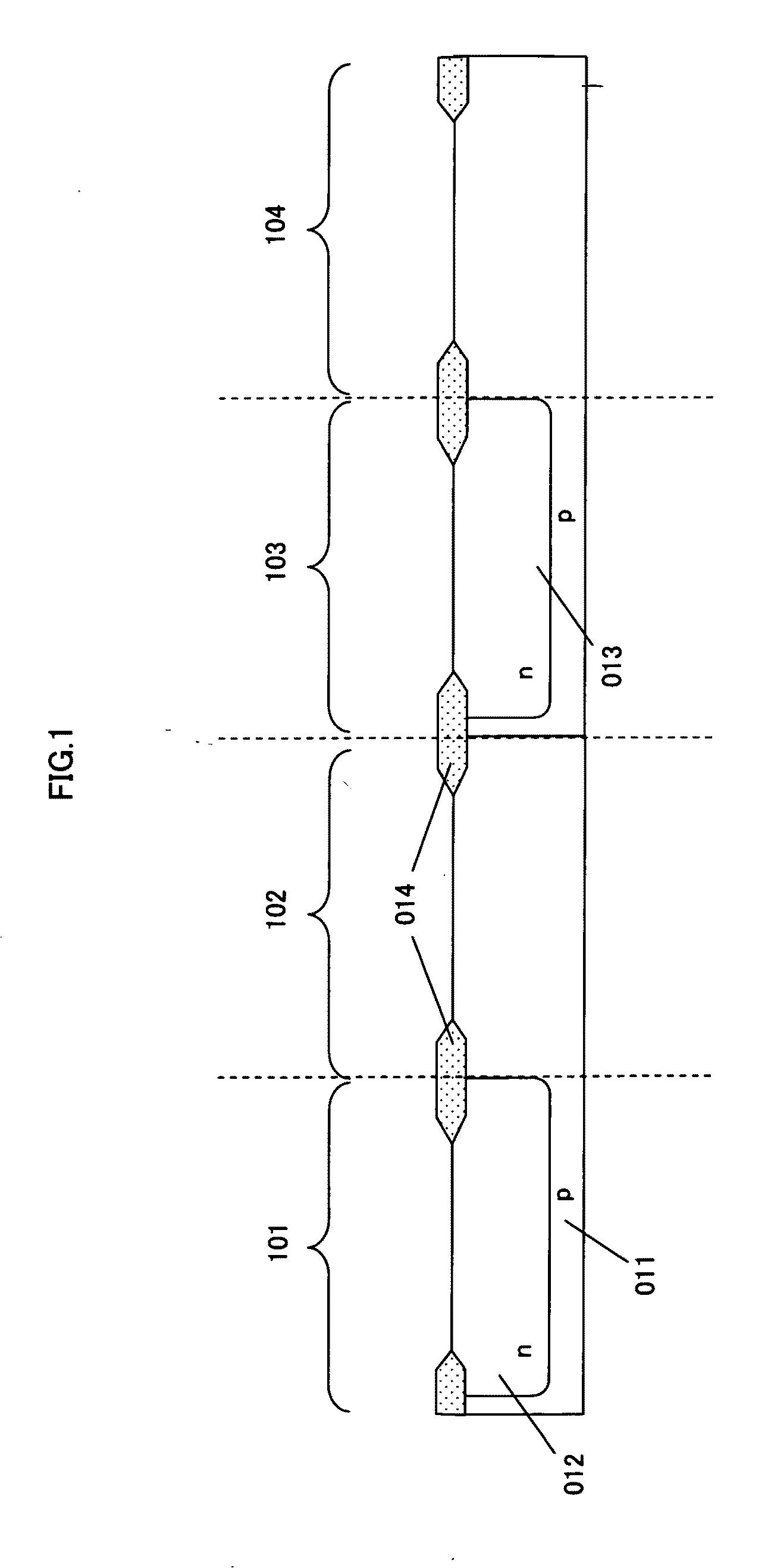
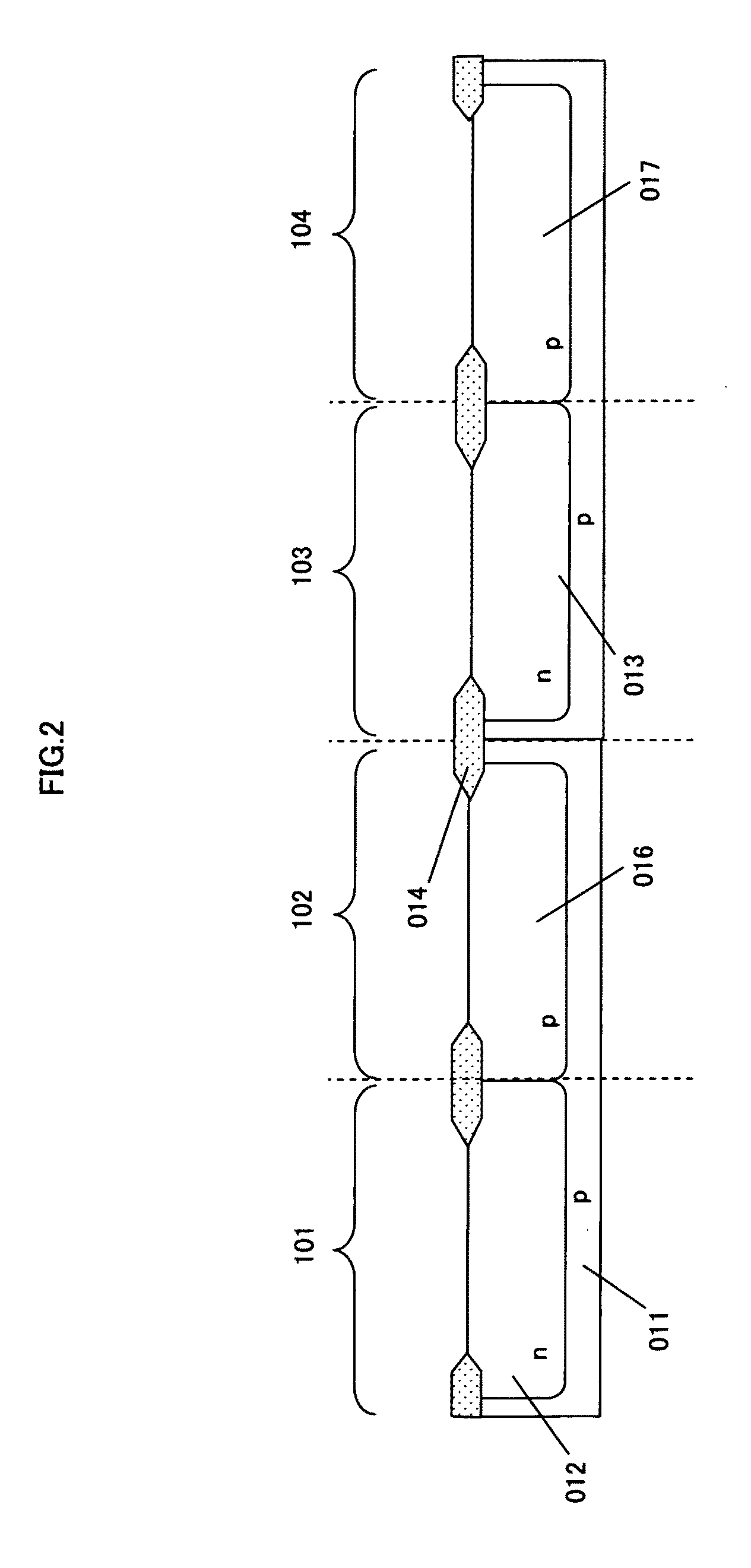
[0058]FIG. 1 to FIG. 10 are sectional views each showing a semiconductor device in a process under manufacture.

[0059]The following describes the manufac...

second embodiment

[0116]The following describes a semiconductor device relating to a second embodiment of the present invention, with reference to the drawings.

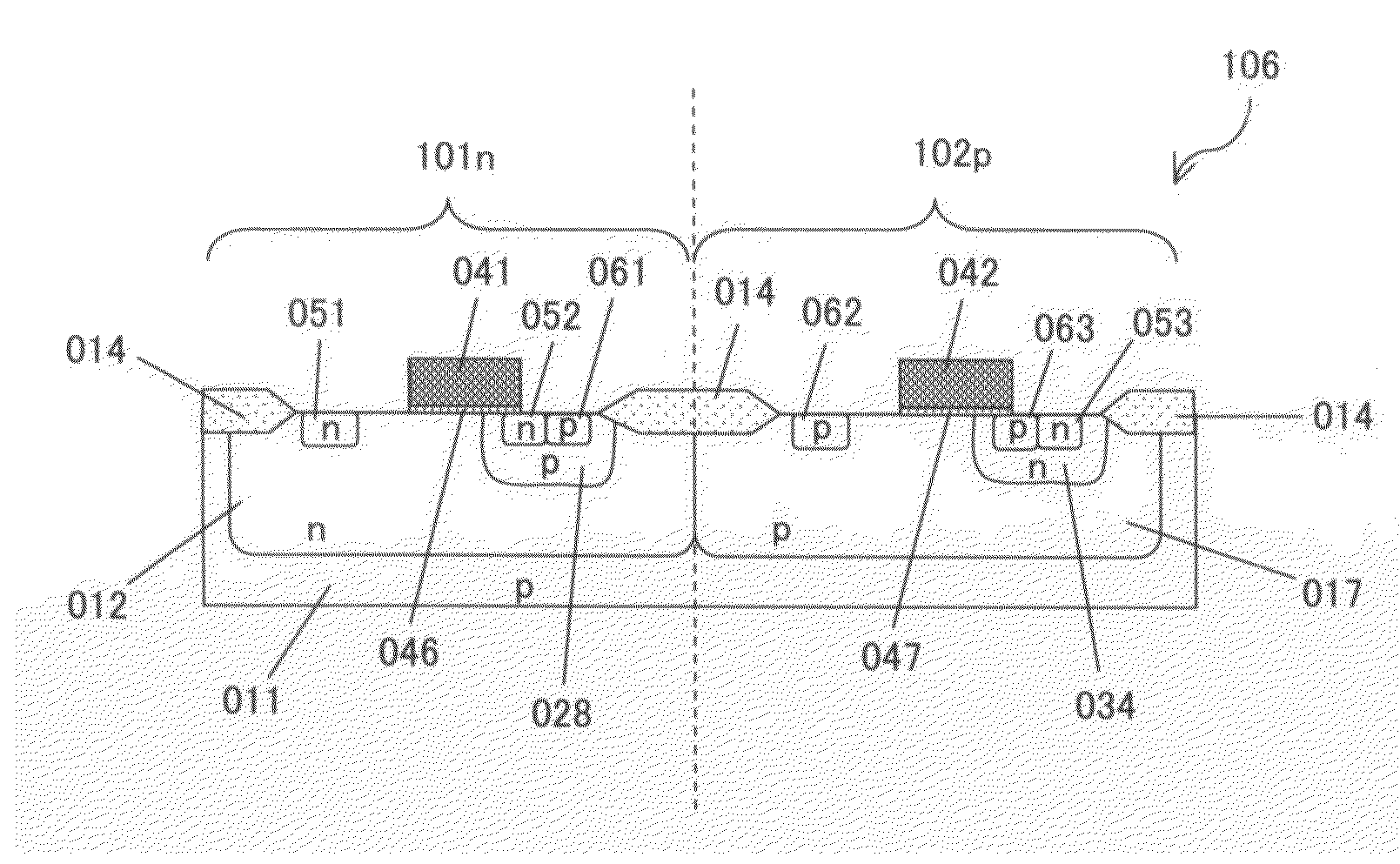
[0117]FIG. 11 is a sectional view showing the semiconductor device relating to the second embodiment. The semiconductor device includes a complementary LDMOS transistor 106, as shown in FIG. 11. The complementary LDMOS transistor 106 shown in

[0118]FIG. 11 is part of a semiconductor device manufactured by the manufacturing method relating to the first embodiment, which has referential numerals that are the same as those in the figures used for describing the first embodiment.

[0119]The complementary LDMOS transistor 106 is composed of an n-channel LDMOS transistor 101n and a p- channel LDMOS transistor 102p that are formed in the same semiconductor substrate 011. The n-channel LDMOS transistor 101n and the p-channel LDMOS transistor 102p are electrically disconnected with each other via an isolation insulator film 014.

[0120]The n-channel LDMOS t...

third embodiment

[0127]The following describes a semiconductor device relating to a third embodiment of the present invention, with reference to the drawings.

[0128]FIG. 12 is a sectional view showing a complementary LDMOS transistor 107 of the semiconductor device relating to the third embodiment.

[0129]As shown in FIG. 12, the complementary LDMOS transistor 107 has an insulator film between the gate electrode and the drain diffusion layer in the semiconductor device relating to the second embodiment. In FIG. 12, elements of the complementary LDMOS transistor 107 that are the same as those of the complementary LDMOS transistor 106 have the same numerical references.

[0130]The complementary LDMOS transistor 107 is composed of an n-channel LDMOS transistor 108n and a p-channel LDMOS transistor 109p.

[0131]The n-channel LDMOS transistor 108n has substantially the same structure as that of the n-channel LDMOS transistor 101n relating to the second embodiment. However, the n-channel LDMOS transistor 108n d...


PUM


Abstract

A manufacturing method of a semiconductor device including an LDMOS transistor includes: a process (a) of forming a first conductive well diffusion layer in the semiconductor substrate; a process (b) of sequentially forming a gate insulator film, a gate conductive film, and a photoresist film on a region on the semiconductor substrate corresponding to the well diffusion layer; a process (c) of performing photolithography to remove a part of the photoresist film formed in a predetermined region, and etching the gate conductive film using a remaining part of the photoresist film as a mask so as to form an opening in the predetermined region; a process (d) of doping second conductive impurity ions using a remaining part of the gate conductive film and the remaining part of the photoresist film as a mask so as to form the body layer; and a process (e) of removing the remaining part of the gate conductive film except a part corresponding to the gate electrode formed based on a part that constitutes a lateral surface of the gate conductive film facing the opening.

Description

[0001]This disclosure of Japanese Patent Application No. 2009-015909 filed Jan. 27, 2009 including specification, drawings and claims is incorporated herein by reference in its eternity.BACKGROUND OF THE INVENTION[0002](1) Field of the Invention[0003]The present invention relates to a manufacturing method of a semiconductor device that includes an LDMOS transistor.[0004](2) Related Art[0005]With recent high integration of semiconductor integrated circuit devices, there arises a demand for semiconductor integrated circuit devices including a high voltage LDMOS (Laterally Diffused Metal Oxide Semiconductor) element, a low voltage CMOS (Complementary Metal Oxide Semiconductor) element, a bipolar element, and the like that are integrated in the same substrate. An LDMOS transistor that is an example of the high voltage LDMOS element is demanded to have less power consumption and size for mobile apparatuses. Furthermore, such an LDMOS transistor is demanded to include other element having...

Claims


Application Information

Patent Timeline
Patent Type & Authority Applications(United States)
IPC IPC(8): H01L29/78H01L21/336H01L21/8238
CPCH01L21/26586H01L21/823814H01L29/7816H01L29/42368H01L21/823857
Inventor KOBAYASHI, YASUSHIINOUE, MASAKIMIYAGAWA, KOHEI
Owner PANASONIC CORP
Why Eureka
Try Eureka