
Semiconductor device
a semiconductor and device technology, applied in the field of objects, can solve the problems of inability to achieve mobility which is necessary and sufficient, inability to achieve mobility, and inability to achieve high speed operation, etc., and achieve the effects of low cost, high speed and low power
- Summary
- Abstract
- Description
- Claims
- Application Information
AI Technical Summary
Benefits of technology
Problems solved by technology
Method used
Image

Examples
embodiment modes
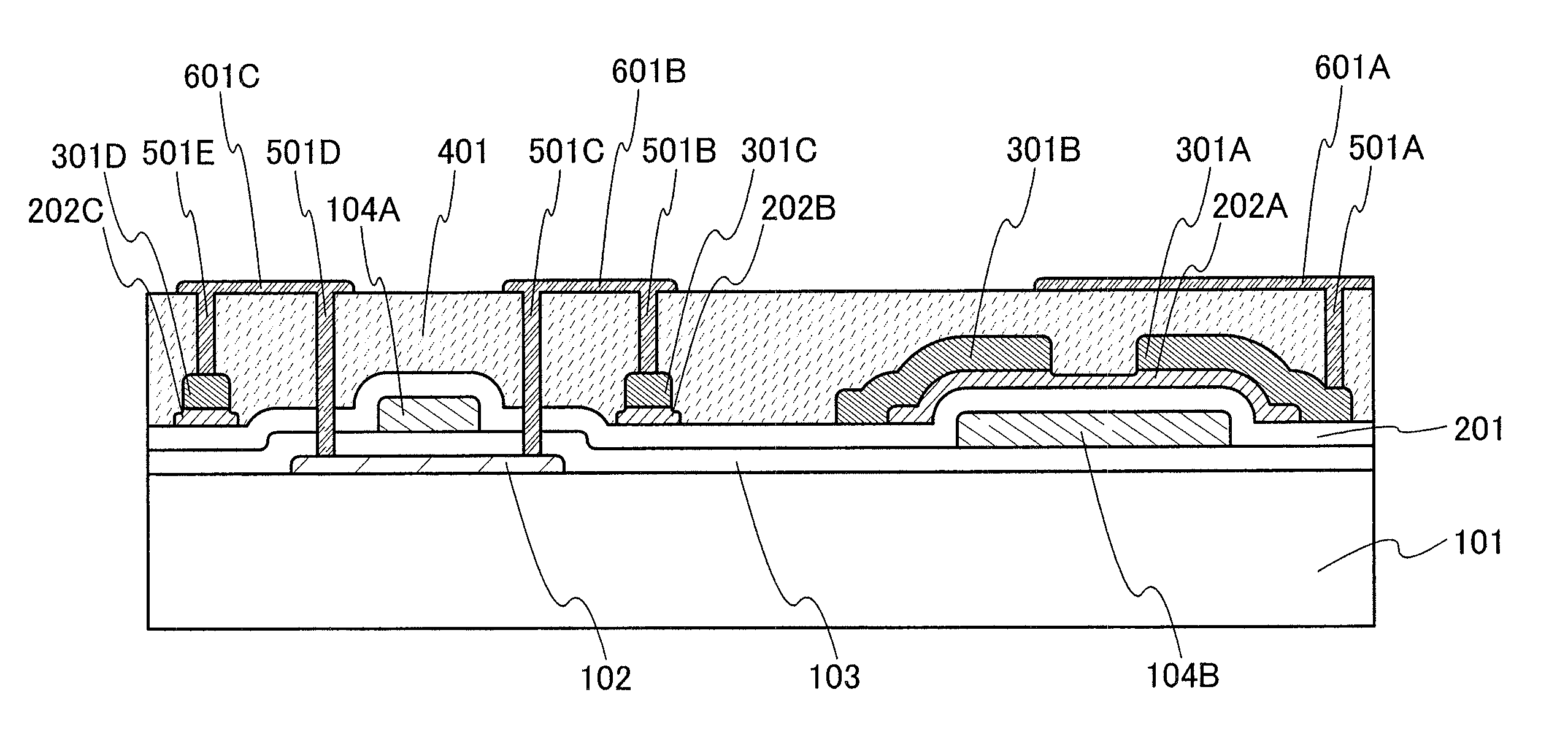
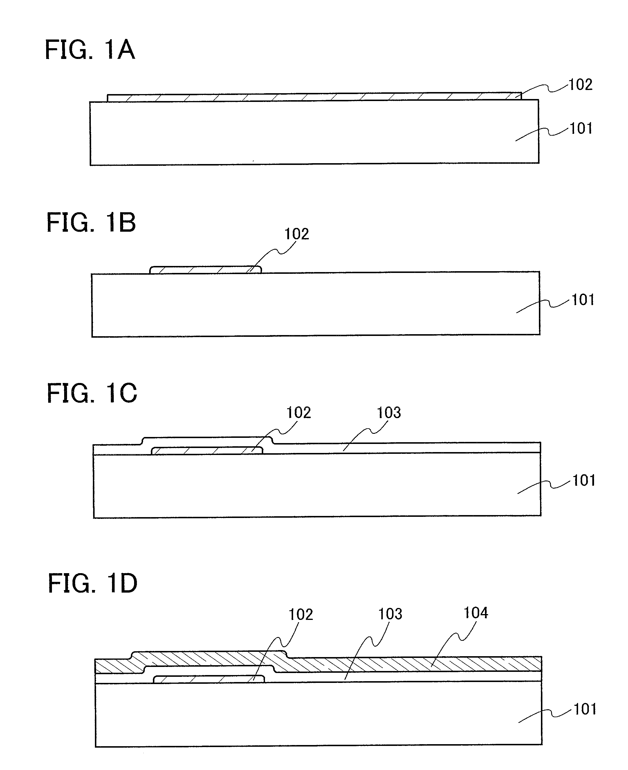
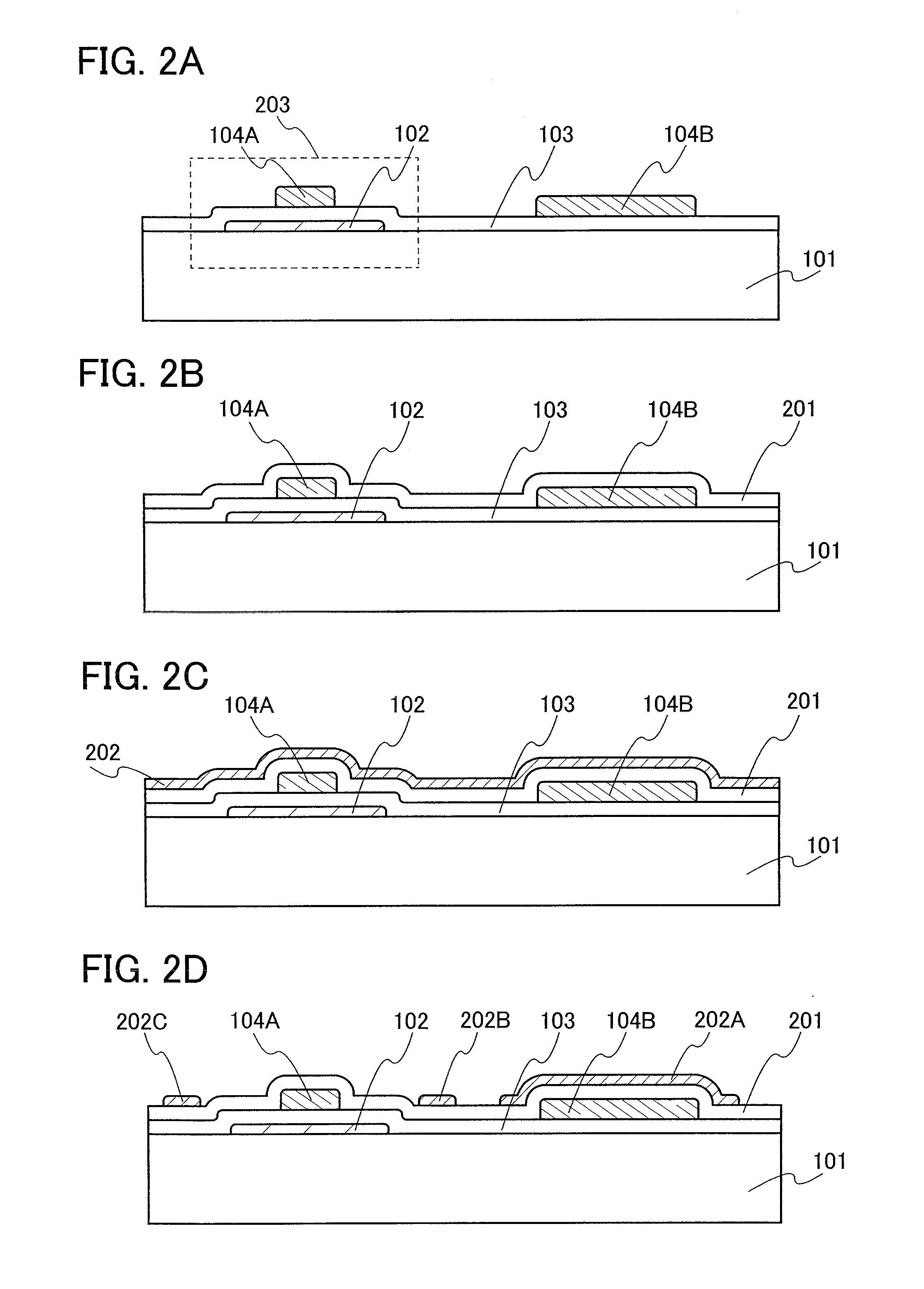
[0133]Embodiment Modes of the present invention will be hereinafter described in detail with reference to the accompanying drawings. However, it is easily understood by those skilled in the art that the present invention can be implemented in various different modes, and modes and details of the present invention can be modified in various ways without departing from the purpose and the scope of the present invention. Accordingly, the present invention should not be interpreted as being limited to the description of the embodiment modes. Note that in structures of the present invention described below, reference numerals denoting the same components are used in common in different drawings, and detailed description of the same portions or portions having similar functions is omitted.
embodiment mode 1
[0134]All or a part of a semiconductor device or a display device includes a TFT which is formed over a glass substrate in such manner that a silicon layer is separated from a single-crystal substrate and bonded (transferred) to the glass substrate, or a TFT formed over a glass substrate in such a manner that a single-crystal substrate is bonded to the glass substrate and separated from the glass substrate to form a silicon layer over the glass substrate. Not that the TFTs which is formed over a glass substrate in such manner that a silicon layer is separated from a single-crystal substrate and transferred to the glass substrate, or a TFT formed over a glass substrate in such a manner that a single-crystal substrate is bonded to a glass substrate and separated from the glass substrate to transfer a silicon layer which is part of the silicon substrate over the glass substrate are hereinafter referred to as single-crystal TFT.
[0135]Then, a non-single-crystal TFT is also formed at the ...
embodiment mode 2
[0210]Next, an arranging method of the semiconductor layer used for the single-crystal TFT is described.
[0211]FIGS. 12A and 12B show an SOI substrate of the present invention. In FIG. 12A, a base substrate 9200 is a substrate having an insulating surface or an insulating substrate, and a variety of glass substrates that are used in the electronics industry, such as aluminosilicate glass, aluminoborosilicate glass, or barium borosilicate glass, can be used. Alternatively, a quartz glass substrate or a semiconductor substrate such as a silicon wafer can be used. An SOI layer 9202 is a single-crystal semiconductor, and single-crystal silicon is typically applied thereto. Alternatively, a semiconductor layer which is separated from a single-crystal semiconductor layer or a polycrystal semiconductor layer of silicon or germanium using a hydrogen ion implantation separation method can be applied. Alternatively, crystalline semiconductor layer formed by using a compound semiconductor such ...
PUM
 Abstract
Description
Claims
Application Information