Phosphor, method for producing the same and light-emitting device using the same

a technology of phosphor and light-emitting device, applied in the field of phosphor, can solve the problems of color rendering becoming ununiform, light emission brightness impairment, and impaired brightness of phosphor, and achieve excellent stability, high light emission intensity, and high brightness

Active Publication Date: 2010-08-12
NAT INST FOR MATERIALS SCI
View PDF12 Cites 99 Cited by
  • Summary
  • Abstract
  • Description
  • Claims
  • Application Information

AI Technical Summary

Benefits of technology

[0101]According to the above-described configuration, in which a phosphor having a brightness higher than the phosphor in the related art, and having excellent stability are illustrated, a method for producing and light-emitting device using it can be provided.
[0102]The phosphor according to the invention has a composition represented by a general formula: M(0)aM(1)bM(2)x−(vm+n)M(3)(vm+n)−yOnNz−n, wherein M(0) is one or more elements selected from Li, Na, Be, Mg, Ca, Sr, Ba, Sc, Y, La, Gd and Lu; M(1) is one or more activators selected from Mn, Ce, Pr, Nd, Sm, Eu, Tb, Dy, Ho, Er, Tm and Yb; M(2) is one or more elements selected from Si, Ge, Sn, Ti, Hf and Zr; M(3) is one or more elements selected from Be, B, Al, Ga, In, Ti and Zn; O is oxygen; N is nitrogen; and the atomic ratio of M(0), M(1), M(2), M(3), O and N is adjusted to satisfy the following: x, y and z satisfy 33≦x≦51, 8≦y≦12 and 36≦z≦56; a and b satisfy 3≦a+b≦7 and 0.001≦b≦1.2; m and n satisfy 0.8·me≦m≦1.2·me and 0≦n≦7 in which me=a+b; and v satisfies v={a·v(0)+b·v(1)} / (a+b) (wherein v(0) is a valence of M(0) ion and v(1) is a valence of M(1) ion). With this configuration, light emitting intensity with sufficiently high brightness can be provided.
[0103]The phosphor according to the invention is formed of the phosphor described above and other materials. The phosphor described above is included in an amount of not less than 80% by volume. The remainder is one or more materials selected from β-sialon, unreacted silicon nitride or aluminum nitride, oxynitride glass, SrSiAl2N2O3, Sr2Al2Si10N14O4, SrSi(10−n)Al(18+n)OnN(32−n) (n˜1) and SrSi6N8. With this configuration, a sufficiently high light emitting intensity is obtained.
[0104]The phosphor according to the invention is powder having an average particle diameter of not less than 0.1 μm to not more than 50 μm. Accordingly, the phosphor is free of influence regarding surface defects. Absorption of excitation light of the phosphor is sufficient and high-intensity light emission is thus obtained.
[0105]In the phosphor according to the invention, an average aspect ratio of primary particles constituting the phosphor is not more than 20. Such an average aspect ratio provides increased dispersibility of the phosphor to resin, an efficient absorption of excitation light and a sufficiently high light emitting intensity.
[0106]The phosphor according to the invention includes a small amount of fluorine and boron as impurities. Light emitting intensity is further increased.

Problems solved by technology

In the light-emitting devices using related art phosphors, such as silicate phosphor, phosphate phosphor, aluminate phosphor and sulfide phosphor, however, there has been a problem that brightness of the phosphor is impaired when exposed to the excitation sources described above.
Regarding light-emitting devices, such as lighting, there is a problem that a white light emitting diode formed by a blue light emitting diode device and an yttrium aluminum garnet-based phosphor is characterized by emitting bluish white light due to shortage of a red component and thus the color rendering becomes ununiform.
Accordingly, there has been a problem that light emission brightness is impaired due to an increase in the heat generation rate of a high-brightness semiconductor light-emitting device.
A sulfide-based phosphor is known to have high light emission brightness, but is chemically unstable.
It is therefore difficult to provide a long-life characteristic inherent to a white LED.

Method used


Image

  • Phosphor, method for producing the same and light-emitting device using the same
  • Phosphor, method for producing the same and light-emitting device using the same
  • Phosphor, method for producing the same and light-emitting device using the same

Examples


first embodiment

[0254]As a first embodiment of the light-emitting device according to the invention, a round-type white light emitting diode lamp (i.e., a LED lighting device or a LED device) will be described.

[0255]FIG. 1 is a cross-sectional view of a round-type white light emitting diode lamp 1 which is the first embodiment of the light-emitting device according to the invention.

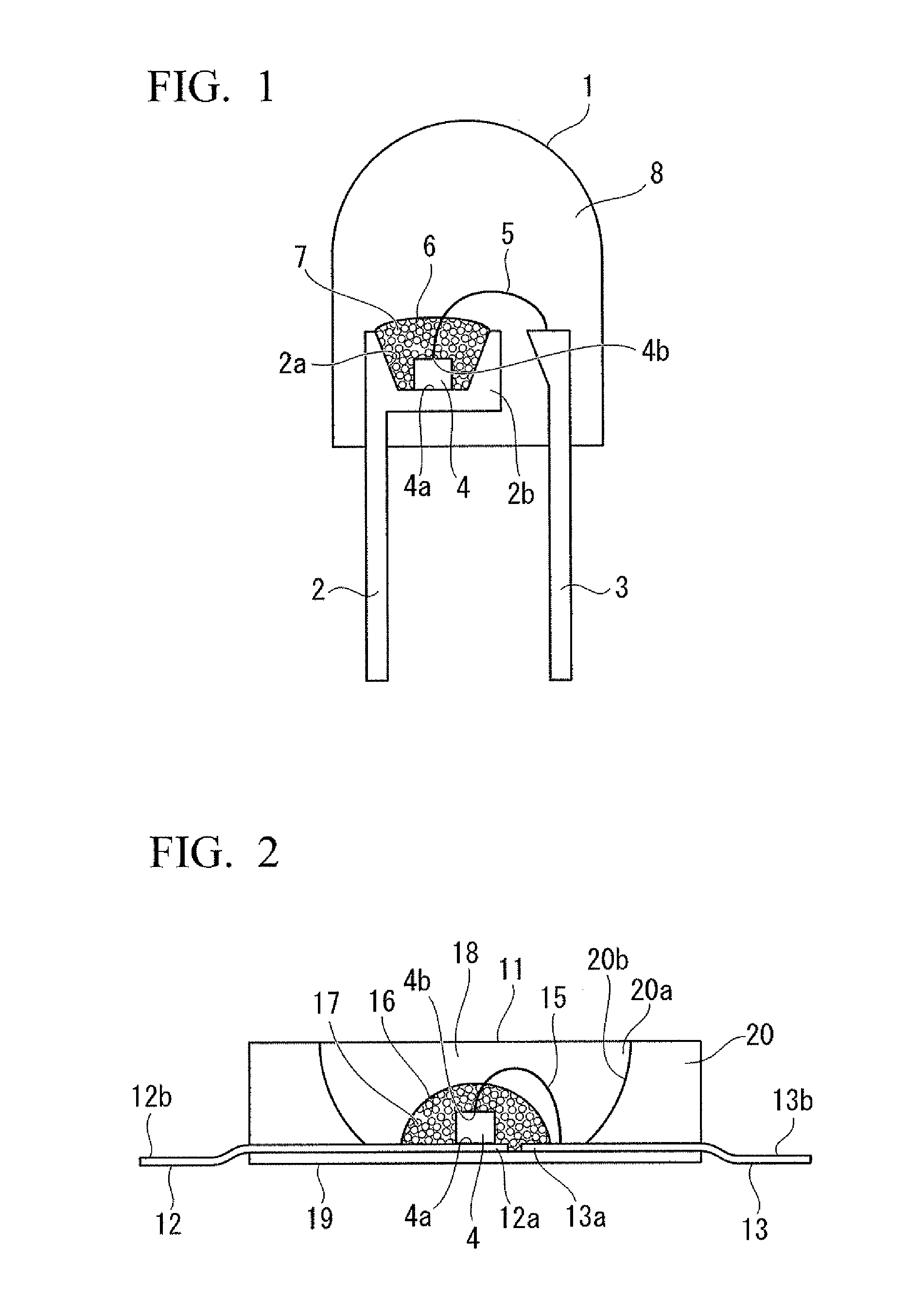
[0256]As illustrated in FIG. 1, the round-type white light emitting diode lamp 1 includes a first lead wire 2 and a second lead wire 3. The first lead wire 2 includes a recess 2a, in which a light emitting diode device (i.e., a LED chip) 4 is placed. A lower electrode 4a of the light emitting diode device 4 is electrically connected to a bottom surface of the recess 2a with conductive paste. An upper electrode 4b of the light emitting diode device 4 is electrically connected to a second lead wire 3 by a bonding wire (i.e., a fine gold wire) 5.

[0257]A first resin (i.e., sealing resin) 6 is a transparent resin in which a p...

second embodiment

[0263]As a second embodiment of the light-emitting device according to the invention, a chip-type white light emitting diode lamp (i.e., a LED lighting device or a LED device) will be described.

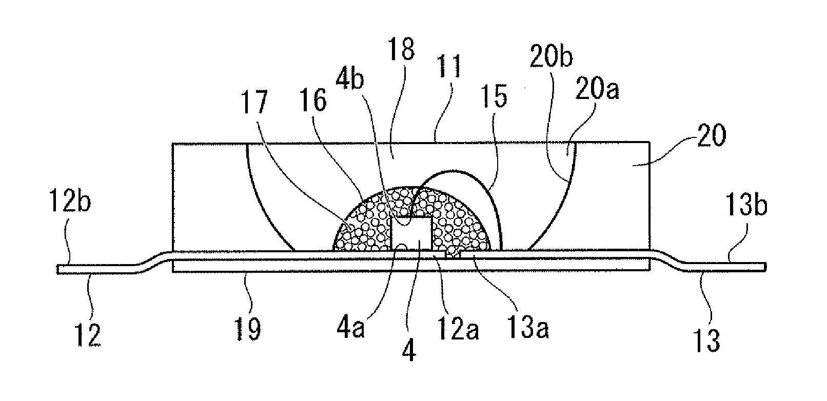
[0264]FIG. 2 is a cross-sectional view of a chip-type white light emitting diode lamp 11 which is the second embodiment of the light-emitting device according to the invention.

[0265]As illustrated in FIG. 2, in the chip-type white light emitting diode lamp 11, a first lead wire 12 and a second lead wire 13 are fixed to a ceramic substrate 19, which is made of alumina ceramic having a high light reflectance. A first end 12a of the first lead wire 12 and a first end 13a of the second lead wire 13 are positioned at a substantially central portion of the substrate 19. A second end 12b of the first lead wire 12 and a second end 13b of the second lead wire 13 are drawn out of the substrate 19 to form electrodes to be soldered when the substrate 19 is mounted on an electric substrate. A light emitti...

third embodiment

[0272]As a second embodiment of the light emitting device according to the invention, a chip-type white light emitting diode lamp for mounting a substrate (i.e., a LED lighting device or a LED device) will be described.

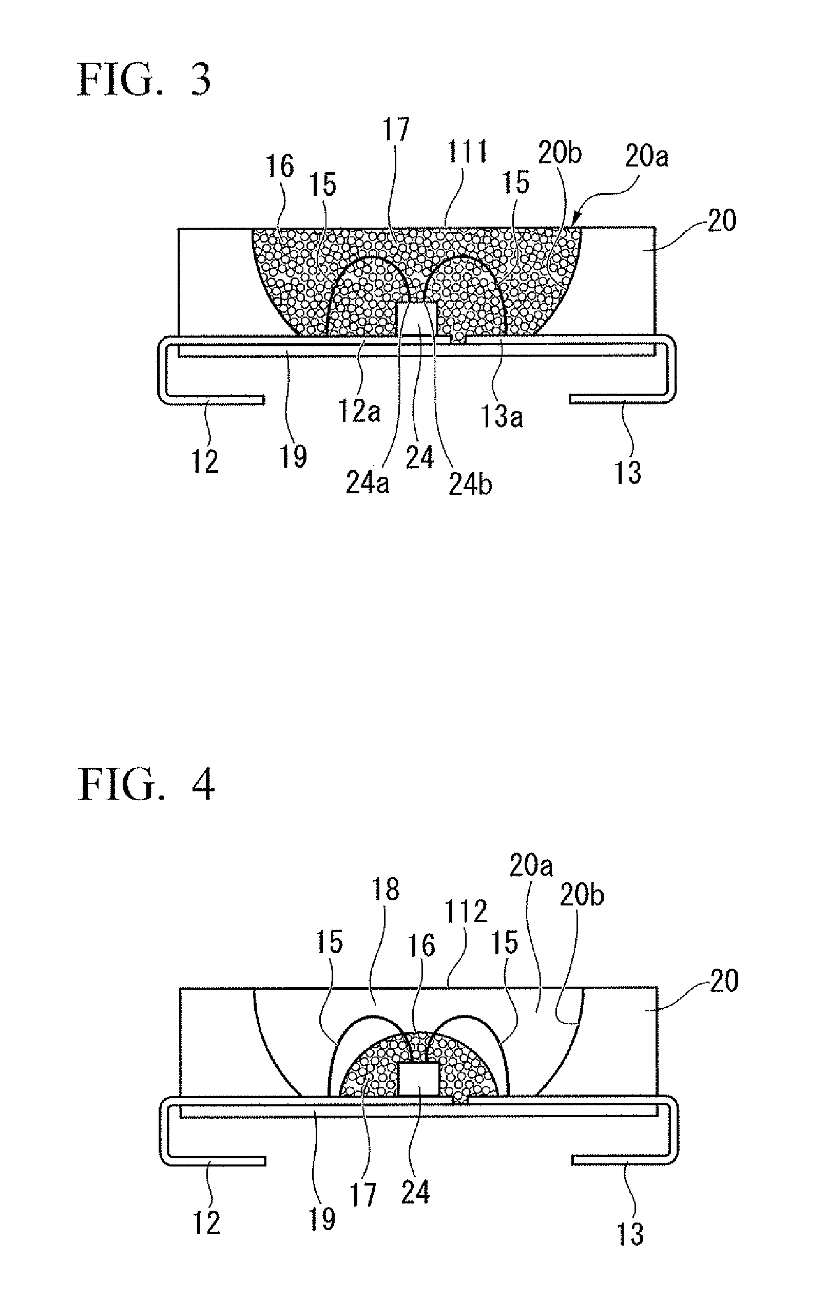
[0273]FIG. 3 is a cross-sectional view of a chip-type white light emitting diode lamp 111 for mounting a substrate which is the third embodiment of the light-emitting device according to the invention.

[0274]As illustrated in FIG. 3, in the chip-type white light emitting diode lamp 111, a first lead wire 12 and a second lead wire 13 are fixed to a ceramic substrate 19, which is made of alumina ceramic having high light reflectance. A first end 12a of the first lead wire 12 and a first end 13a of the second lead wire 13 are positioned at a substantially central portion of the substrate 19. Another end 12b of the first lead wire 12 and another end 13b of the second lead wire 13 are drawn out of the substrate 19 to form electrodes to be soldered when the substrate 19 is m...


PUM


Abstract

The invention is a phosphor which includes a phosphor material having a composition represented by a general formula: M(0)aM(1)bM(2)x−(vm+n)M(3)(vm+n)−yOnNz−n, wherein M(0) is one or more elements selected from Li, Na, Be, Mg, Ca, Sr, Ba, Sc, Y, La, Gd and Lu; M(1) is one or more activators selected from Mn, Ce, Pr, Nd, Sm, Eu, Tb, Dy, Ho, Er, Tm and Yb; M(2) is one or more elements selected from Si, Ge, Sn, Ti, Hf and Zr; M(3) is one or more elements selected from Be, B, Al, Ga, In, Tl and Zn; O is oxygen; N is nitrogen; and an atomic ratio of M(0), M(1), M(2), M(3), O and N is adjusted to satisfy the following: x, y and z satisfy 33≦x≦51, 8≦y≦12 and 36≦z≦56; a and b satisfy 3≦a+b≦7 and 0.001≦b≦1.2; m and n satisfy 0.8·me≦m≦1.2·me and 0≦n≦7 in which me=a+b; and v satisfies v={a·v(0)+b·v(1)} / (a+b) (wherein v(0) is a valence of M(0) ion and v(1) is a valence of M(1) ion). The invention also relates to a method for producing the phosphor and a light-emitting device using the phosphor.

Description

TECHNICAL FIELD[0001]The present invention relates to a phosphor consisting mainly of an inorganic compound and usage thereof. More particularly, the usage relates to light-emitting devices, such as a lighting device and a display device which uses a property of the phosphor, i.e., property of emitting fluorescent light at a wavelength of not less than 400 nm.BACKGROUND ART[0002]Generally, a phosphor is used in light-emitting devices of display devices such as a vacuum fluorescent display (VFD), a field emission display (FED), a plasma display panel (PDP), a cathode-ray tube (CRT) and a light emitting diode (i.e., a LED device).[0003]In these light-emitting devices, it is necessary to supply certain energy to the phosphor in order to excite the phosphor and cause the phosphor to emit light. The phosphor is excited by an excitation source with high energy, such as a vacuum ultraviolet ray, an ultraviolet ray, an electron ray or a blue light and is caused to emit visible light.[0004]I...

Claims


Application Information

Patent Timeline
Patent Type & Authority Applications(United States)
IPC IPC(8): H01L33/44H01L33/48H01J1/62C09K11/79B05D5/12C09K11/08C09K11/59C09K11/64C09K11/66C09K11/67C09K11/80H01L33/50H01L33/54H01L33/56H01L33/60H01L33/62
CPCC09K11/0883C09K11/7734H01L33/502H05B33/14H01L2224/45144H01L2224/8592H01L2224/48247H01L2224/48091H01L2224/48257C09K11/592H01L2924/00014H01L2924/00H01L24/45H01L2924/12042H01L2924/12041C09K11/77348
Inventor SHIOI, KOUSUKEHIROSAKI, NAOTOMIKI, HISAYUKI
Owner NAT INST FOR MATERIALS SCI
Why Eureka
Try Eureka