Field emission display and manufacturing method of the same having selective array of electron emission source

a manufacturing method and field emission technology, applied in the manufacture of electrode systems, electric discharge tubes/lamps, discharge tubes luminescnet screens, etc., can solve the problems of reducing the reliabilities and performances of elements, high operating voltage of them, and large leakage current, so as to improve the uniformity of pixels, reduce the production cost, and simplify the manufacturing process of fed

Inactive Publication Date: 2010-08-12
WORLDBEAM SOLUTIONS CO LTD
View PDF12 Cites 15 Cited by
  • Summary
  • Abstract
  • Description
  • Claims
  • Application Information

AI Technical Summary

Benefits of technology

[0019]As described above, the manufacturing method of FED according to the present invention can decide positions of carbon nano-tubes as electron field emitters such that they are easily formed at the desired positions, before the structure of electrodes is set.
[0020]Also, the present invention can improve uniformity of pixels based on uniform electron emission by forming spacers which can divide electron field emitters into pixel units using photoresist to prevent cross-talks occurring in the operation process of electron field emitters.
[0021]In addition, as stated above, the present invention can realize a FED of big size and a reduction of its production cost at the same time by forming electron field emitters at the desired positions over the lower substrate and using spacers dividing the electron field emitters into pixel units.
[0022]Further, the present invention can simplify the manufacturing process of FED to reduce the cost thereof by forming carbon nano-tubes as electron field emitters without a diffusion barrier layer.
[0023]Also, after forming the desired patterns over a catalytic metal layer by the process of lithography using photoresist, the present invention can form electron field emitters in the desired shapes at the desired positions by growing carbon nano-tubes as electron field emitters on said patterns.
[0024]In addition, the present invention can prevent deterioration of characteristics of carbon nano-tubes, by removing the resist in the place where carbon nano-tubes as electron field emitters are not needed to be grown and thereby reducing the possibility of secondary reaction due to the residual resist.

Problems solved by technology

However, metal tips have problems in that operating voltage of them is very high and leakage current is large due to thermal degradation of the tips resulting from their emitting high currents, and as a result, reliabilities and performances of the elements fall down.
However, the FED using said electron field emitters has problems in that mutual interferences between pixels are occurred and efficiency of electron emission falls down due to the lack of technologies by which carbon nano-tubes can be formed at the desired locations and arrayed vertically.
The emitters for FED which were mainly used in the early developmental stage of said FED had defects in that manufacturing process and structures of them were complicated.
Moreover, since the ion beam of high price was needed to use semi-conductors and metals as electron emission sources, there was another problem that they could not be applied to the FED.

Method used


Image

  • Field emission display and manufacturing method of the same having selective array of electron emission source
  • Field emission display and manufacturing method of the same having selective array of electron emission source
  • Field emission display and manufacturing method of the same having selective array of electron emission source

Examples


Embodiment Construction

[0032]The present invention will now be described more fully with reference to the accompanying drawings, in which exemplary embodiments of the invention are shown.

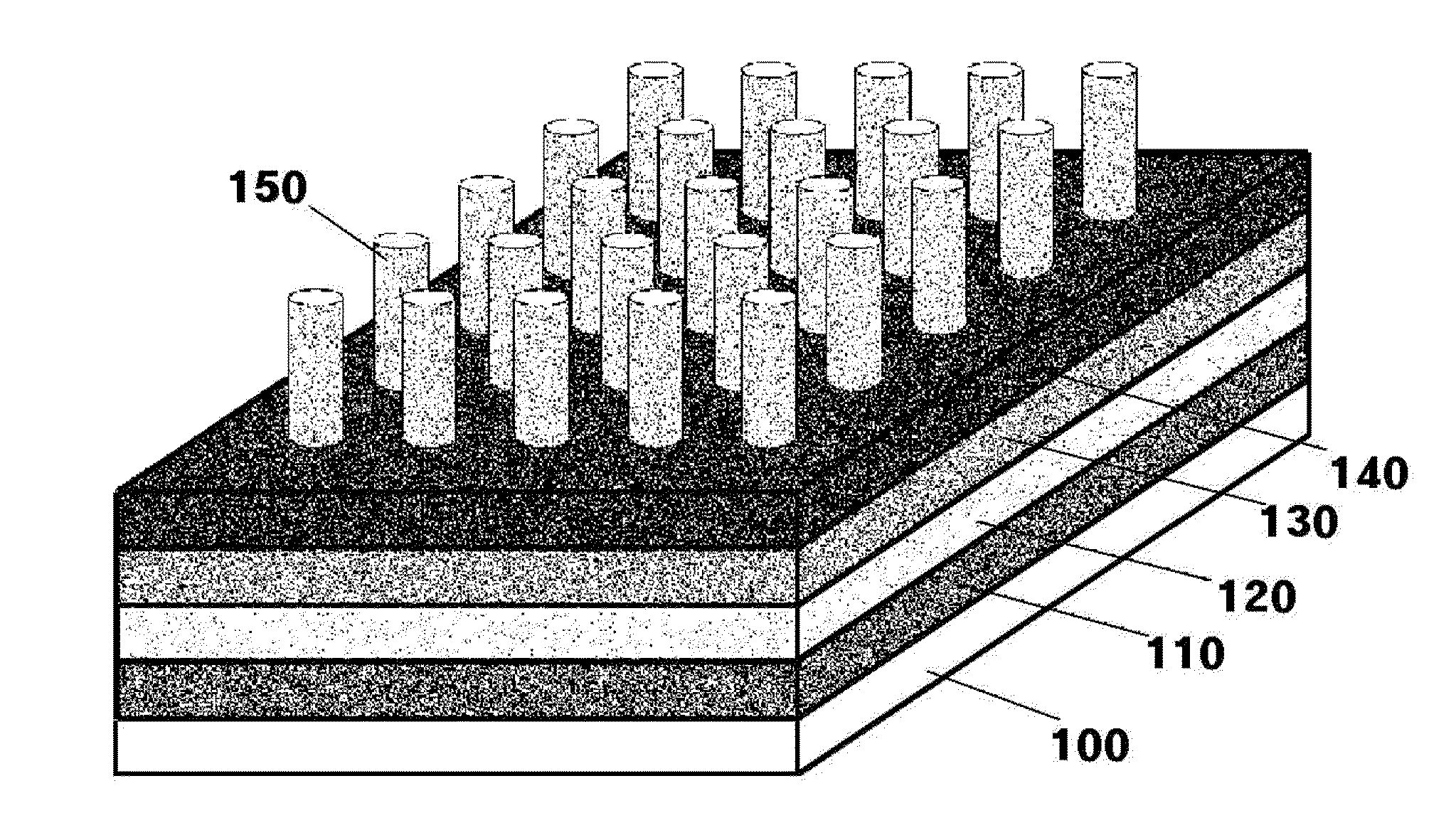
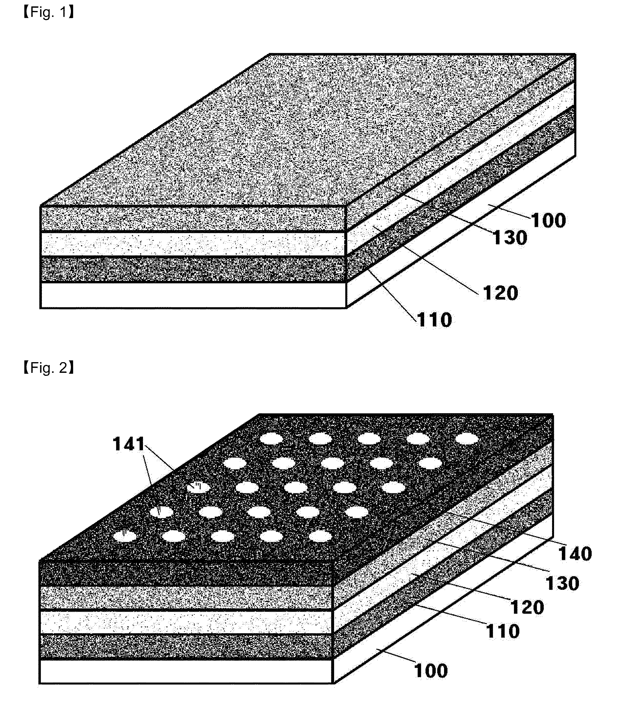
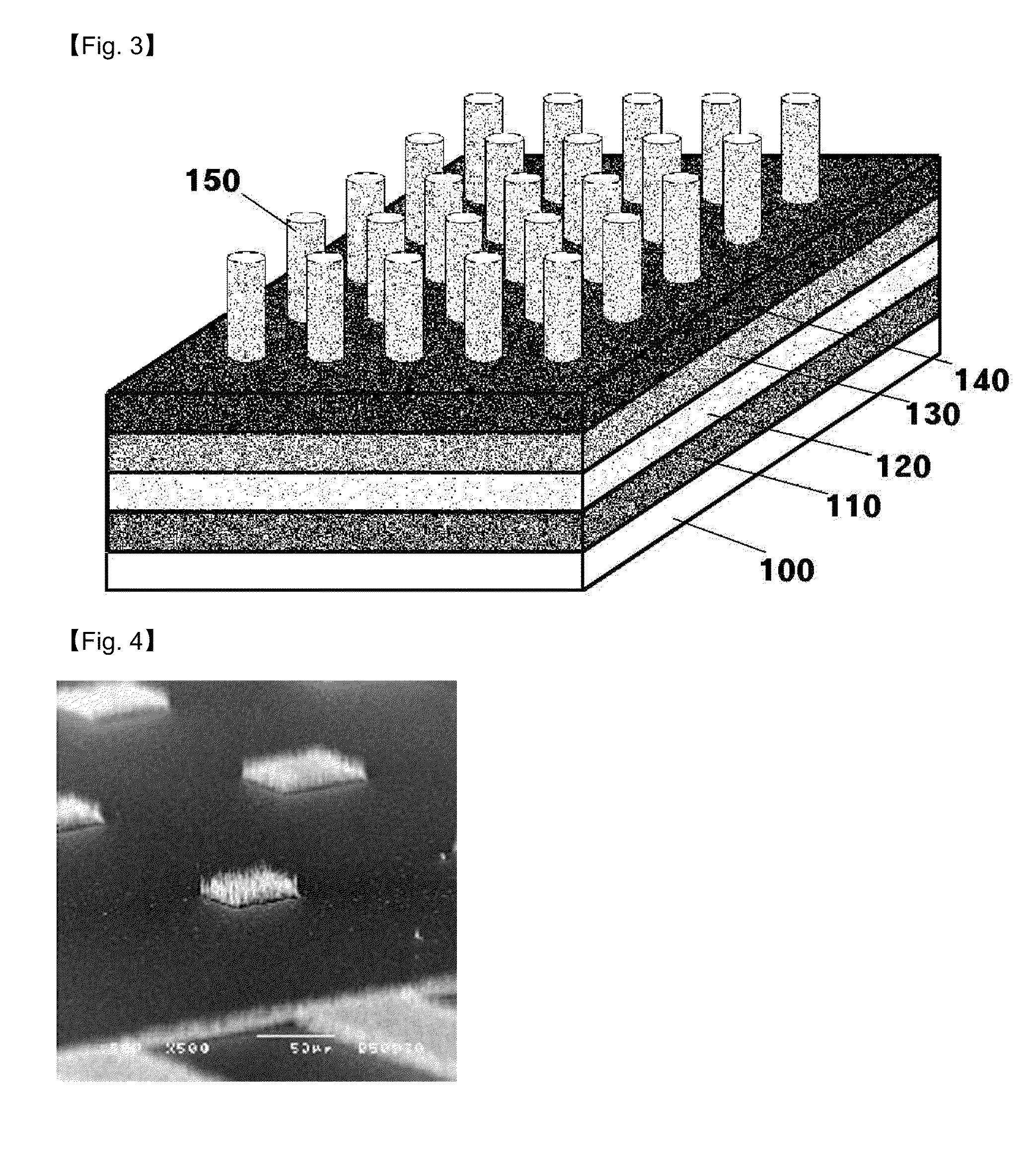
[0033]In the first place, FIGS. 1 through 3 are diagrams sequentially showing the forming method of electron field emitters by selectively growing carbon nano-tubes as electron emission sources at the desired positions using photoresist in the process of lithography, according to an embodiment of the present invention in the manufacturing method of FED.

[0034]Firstly, as shown in FIG. 1, a cathode electrode (110) having a predetermined pattern is formed on a substrate (100) which is composed of one of glass, quartz, silicon or alumina (Al2O3), and then a diffusion barrier layer (120) is formed on said cathode electrode (110) using titanium (Ti) or titanium alloy (Ti-alloy) which is made by mixing titanium with tungsten (W), and etc. Next, a catalyst metal layer (130) is formed on said diffusion barrier layer (120). At this...


PUM


Abstract

The present invention relates to a field emission display and a manufacturing method of the same having selective positioning of electron field emitters. More specifically, the present invention provides a field emission display and a manufacturing method of the same having selective positioning of electron field emitters which can prevent a cross-talk that is a mutual interference phenomenon between pixels and improve uniformity of pixels based on uniform electron emission by deciding positions of carbon nano-tubes which are sources of electron emission and growing carbon nano-tubes before the structure of electrodes is formed, and forming spacers directly on electrodes such that the spacers divide carbon nano-tubes formed uniformly and selectively into pixel units.

Description

TECHNICAL FIELD[0001]The present invention relates to a field emission display and a manufacturing method of the same having selective positioning of electron field emitters. More specifically, the present invention provides a field emission display and a manufacturing method of the same having selective positioning of electron field emitters which can prevent a cross-talk that is a mutual interference phenomenon between pixels and improve uniformity of pixels based on uniform electron emission by deciding positions of carbon nano-tubes which are sources of electron emission and growing carbon nano-tubes before the structure of electrodes is formed, and forming spacers directly on the electrode such that the spacers divide carbon nano-tubes formed selectively and uniformly into pixel units.BACKGROUND ART[0002]In general, a field emission display (FED) is based on electron emission in a vacuum. That is, a FED plays a role of display equipment by making electrons impact to anode elect...

Claims


Application Information

Patent Timeline
Patent Type & Authority Applications(United States)
IPC IPC(8): H01J1/62H01J9/20
CPCB82Y10/00H01J2201/30469H01J31/127H01J9/025
Inventor PARK, KYU CHANGJANG, JINRYU, JE HWANG
Owner WORLDBEAM SOLUTIONS CO LTD
Why Eureka
Try Eureka