Photovoltaic device

a photovoltaic device and photovoltaic technology, applied in the field of photovoltaic devices, can solve the problems of inability to achieve the combination of superior performance and superior solar cell mass productivity, and the rate of deposition is still less than that obtained for deposition using a typical continuous plasma, so as to achieve the effect of improving the efficiency of light absorption and high stability

Inactive Publication Date: 2010-08-19
MITSUBISHI HEAVY IND LTD
View PDF3 Cites 4 Cited by
  • Summary
  • Abstract
  • Description
  • Claims
  • Application Information

AI Technical Summary

Benefits of technology

[0012]The present invention has been developed in light of the above circumstances, and has an object of providing a large surface area photovoltaic device having high conversion efficiency and excellent mass productivity.
[0019]By setting the film thickness of the amorphous silicon i-layer to a value within the above range, light-induced degradation of the photovoltaic device can be suppressed, and a high stabilized output can be achieved.
[0020]In such cases, an intermediate contact layer is preferably provided between the crystalline silicon layer and the amorphous silicon layer. Short wavelength light that is transmitted through the amorphous silicon layer without being completely absorbed is reflected by the intermediate contact layer, thereby lengthening the light path within the amorphous silicon layer and enabling more efficient absorption of the short wavelength light. Further, the intermediate contact layer also improves the contact properties between the crystalline silicon layer and the amorphous silicon layer. As a result, the generated electrical current can be increased without increasing the film thickness of the amorphous silicon layer, meaning a photovoltaic device of high conversion efficiency can be obtained.
[0021]According to the present invention, by ensuring that the Raman peak ratio of the crystalline silicon i-layer has a substrate in-plane distribution described above, a photovoltaic device having high conversion efficiency can be obtained even when the crystalline silicon layer is deposited on a large surface area substrate at a rapid deposition rate in order to improve the productivity.

Problems solved by technology

However, despite the fact that the active species are generated efficiently so that the deposition rate does not decrease as a result of the pulsing, the deposition rate is still less than that obtained for deposition using a typical continuous plasma.
In other words, conventionally there are no techniques available that combine rapid deposition with favorable crystallinity uniformity and film thickness uniformity.
Achieving uniform deposition of a crystalline silicon i-layer within the substrate plane so as to obtain a level of crystallinity that yields superior performance, together with rapid deposition, thereby enabling large surface area solar cell modules comprising a crystalline silicon i-layer to be produced with a combination of superior solar cell mass productivity and superior performance is extremely difficult.
It is known that if the crystallinity of the crystalline silicon i-layer is low, then the sensitivity of the layer to light of longer wavelengths (such as wavelengths of 600 nm or more) deteriorates, causing a decrease in the solar cell performance.

Method used


Image

  • Photovoltaic device
  • Photovoltaic device
  • Photovoltaic device

Examples


example 1

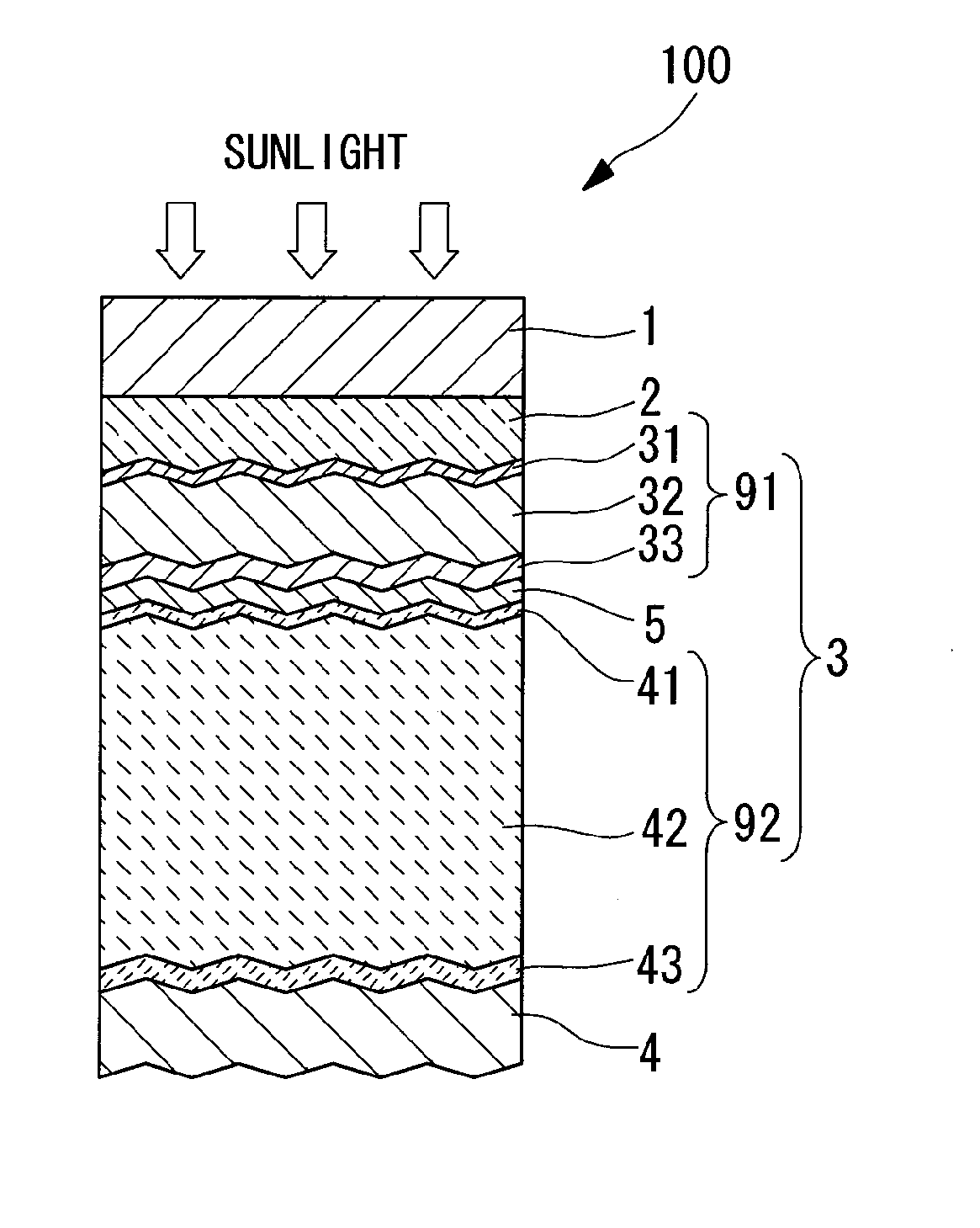
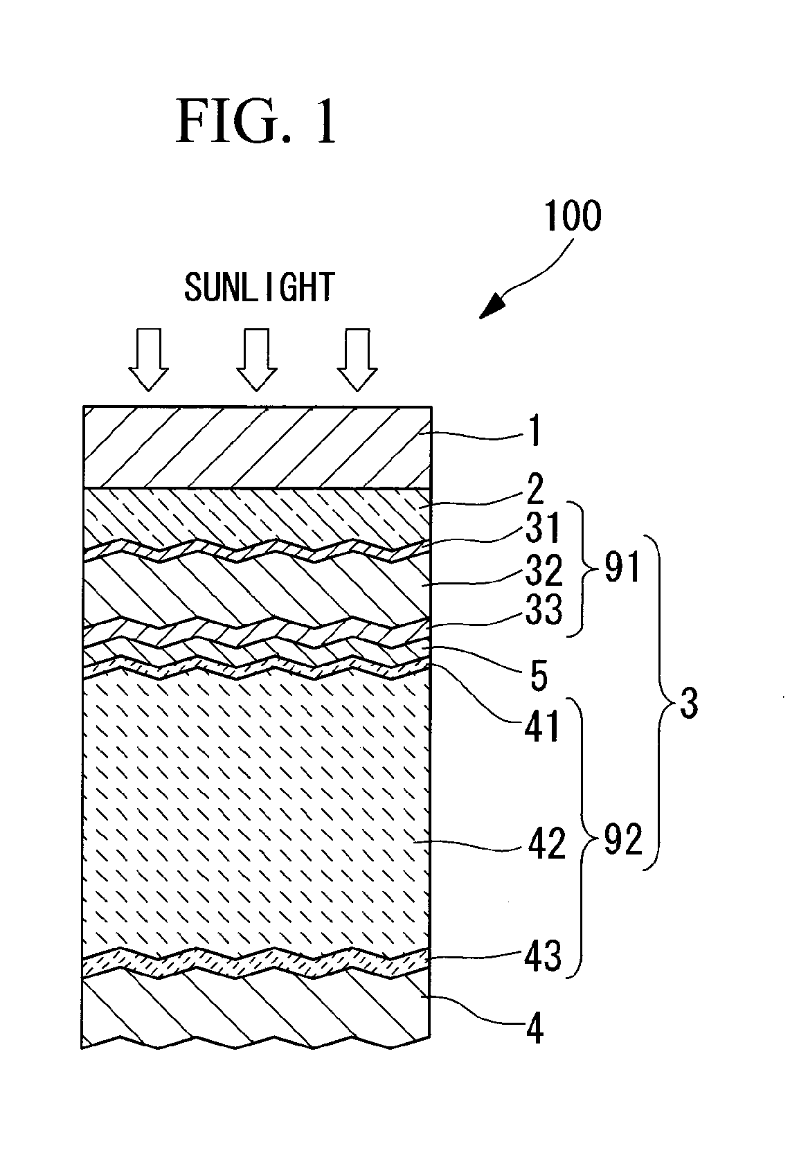
[0077]Using a CVD method, an amorphous silicon layer and a crystalline silicon layer were formed, as the first cell layer 91 and the second cell layer 92 respectively, on a glass substrate of dimensions 1.4 m×1.1 m, thus forming a tandem-type solar cell module. Deposition of the crystalline silicon i-layer 42 was conducted at a deposition rate of 2 nm / sec, and the electric power applied to the plasma electrode and the hydrogen dilution ratio were adjusted appropriately to control the distribution of the Raman peak ratio within the substrate plane.

[0078]Following measurement of the solar cell module output, the substrate was partitioned. Samples were taken from 24 locations within the substrate plane, and following removal of the back electrode layer 4 from each sample by wet etching using hydrogen peroxide (concentration: 30%) and dilute hydrochloric acid (molar concentration: 0.2), the Raman spectrum was measured with the crystalline silicon n-layer 43 exposed at the surface, and t...

example 2

[0082]Using a CVD method, an amorphous silicon layer and a crystalline silicon layer were formed, as the first cell layer 91 and the second cell layer 92 respectively, on a glass substrate of dimensions 1.4 m×1.1 m. Subsequently, the substrate was divided in two, forming tandem-type solar cell modules of dimensions 0.7 m×1.1 m. Deposition of the crystalline silicon i-layer 42 was conducted at a deposition rate of 2 nm / sec, and the applied electric power and the hydrogen dilution ratio were adjusted appropriately to control the crystallinity distribution within the substrate plane.

[0083]Following measurement of the solar cell module output, the substrate was partitioned. The Raman spectrum was measured for samples taken from 24 locations within the substrate plane, and the crystallinity 1c / 1a was determined. Prior to measurement of the Raman spectrum, the back electrode layer 4 was removed from each sample using hydrogen peroxide (concentration: 30%) and dilute hydrochloric acid (mol...

example 3

[0087]Using a CVD method, a first cell layer 91 comprising an amorphous silicon i-layer having a film thickness of 220 nm or 350 nm was formed on a glass substrate of dimensions 1.4 m×1.1 m. In order not to alter the productivity of the solar cell module, the deposition process was adjusted so that the amorphous silicon i-layers were deposited over the same deposition time. A CVD method was then used to form, on top of the first cell layer 91, a second cell layer 92 having a crystalline silicon i-layer of Example 1, for which the Raman peak ratio exhibited a range from 3 to 10, an average value of 6.3 and a standard deviation of 1.7, and for which the proportion of regions having a Raman peak ratio of not more than 4 was 3% or less, thus completing a tandem-type solar cell module.

[0088]Table 3 shows the average film thickness of the amorphous silicon i-layer within the solar cell module, the average film thickness of the crystalline silicon i-layer, and the stabilized output for the...


PUM


Abstract

A large surface area photovoltaic device having high conversion efficiency and excellent mass productivity is provided. A photovoltaic device 100 having a photovoltaic layer 3 comprising a crystalline silicon layer formed on a substrate 1, wherein the crystalline silicon layer has a crystalline silicon i-layer 42, and the crystalline silicon i-layer 42 has a substrate in-plane distribution represented by an average value for the Raman peak ratio, which represents the ratio of the Raman peak intensity for the crystalline silicon phase relative to the Raman peak intensity for the amorphous silicon phase, that is not less than 4 and not more than 8, a standard deviation for the Raman peak ratio that is not less than 1 and not more than 3, and a proportion of regions in which the Raman peak ratio is not more than 4 of not less than 0% and not more than 15%. Also, a photovoltaic device 100 in which the size of the surface of the substrate 1 on which the photovoltaic layer 3 is formed is at least 1 m square, and in which the crystalline silicon i-layer 42 has a substrate in-plane distribution represented by an average value for the Raman peak ratio that is not less than 5 and not more than 8, a standard deviation for the Raman peak ratio that is not less than 1 and not more than 3, and a proportion of regions in which the Raman peak ratio is not more than 4 of not less than 0% and not more than 10%.

Description

TECHNICAL FIELD[0001]The present invention relates to a photovoltaic device, and relates particularly to a photovoltaic device in which the electric power generation layer is formed by deposition.BACKGROUND ART[0002]One known example of a photovoltaic device used in a solar cell that converts the energy from sunlight into electrical energy is a thin-film silicon-based photovoltaic device comprising a photovoltaic layer formed by using a plasma enhanced CVD method or the like to deposit thin films of a p-type silicon-based semiconductor (p-layer), an i-type silicon-based semiconductor (i-layer) and an n-type silicon-based semiconductor (n-layer).[0003]Advantages of thin-film silicon-based solar cells include the comparative ease with which the surface area can be increased, and the fact that the film thickness is approximately 1 / 100th that of a crystalline solar cell, meaning minimal material is required. As a result, thin-film silicon-based solar cells can be produced at lower cost ...

Claims


Application Information

Patent Timeline
Patent Type & Authority Applications(United States)
IPC IPC(8): H01L31/00H01L31/05H01L31/06H01L31/076H01L31/077H01L31/18
CPCH01L31/0236Y02E10/50H01L31/18H01L31/077H01L31/02366Y02E10/547Y02E10/548
Inventor GOYA, SANEYUKISASAKAWA, EISHIROMASHIMA, HIROSHISAKAI, SATOSHI
Owner MITSUBISHI HEAVY IND LTD
Why Eureka
Try Eureka