Switching power source device and drive method thereof
- Summary
- Abstract
- Description
- Claims
- Application Information
AI Technical Summary
Benefits of technology
Problems solved by technology
Method used
Image
Examples
first embodiment
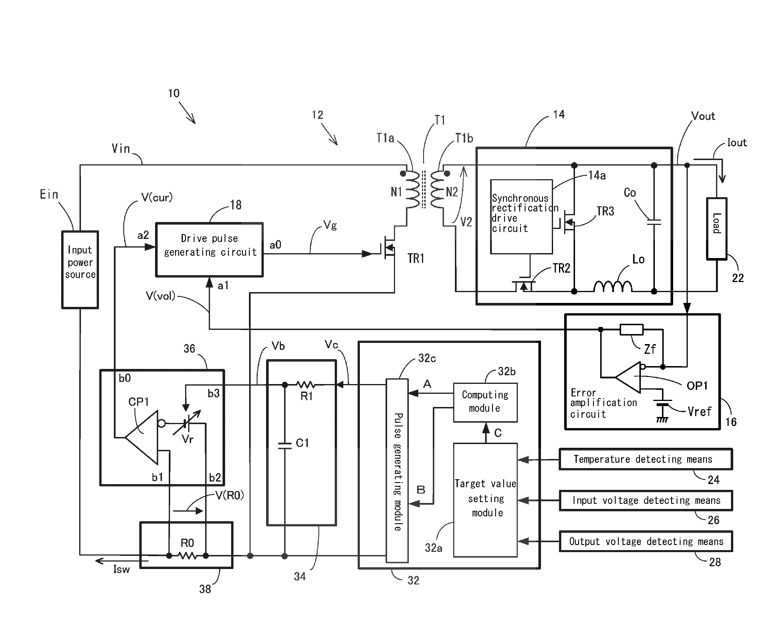
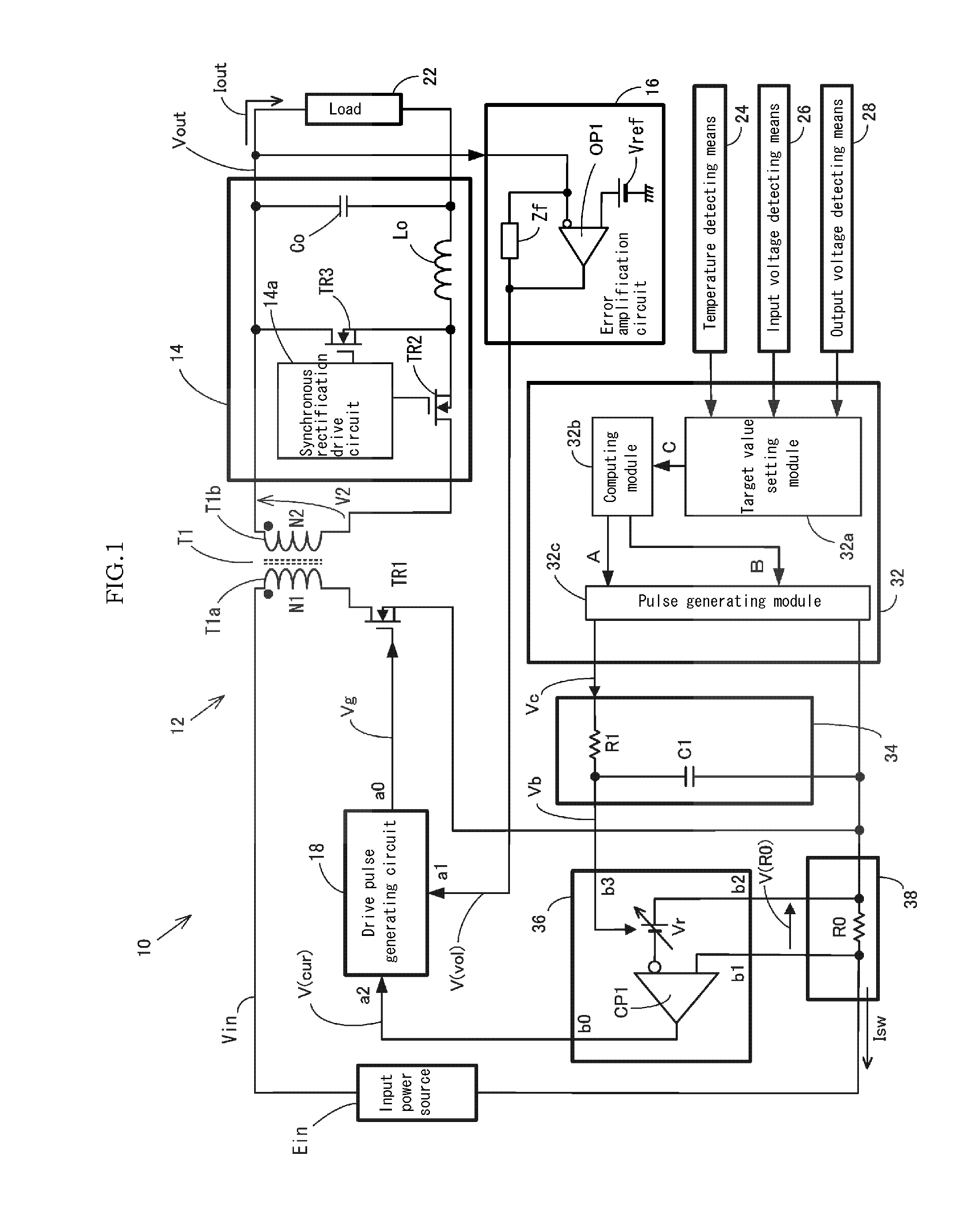
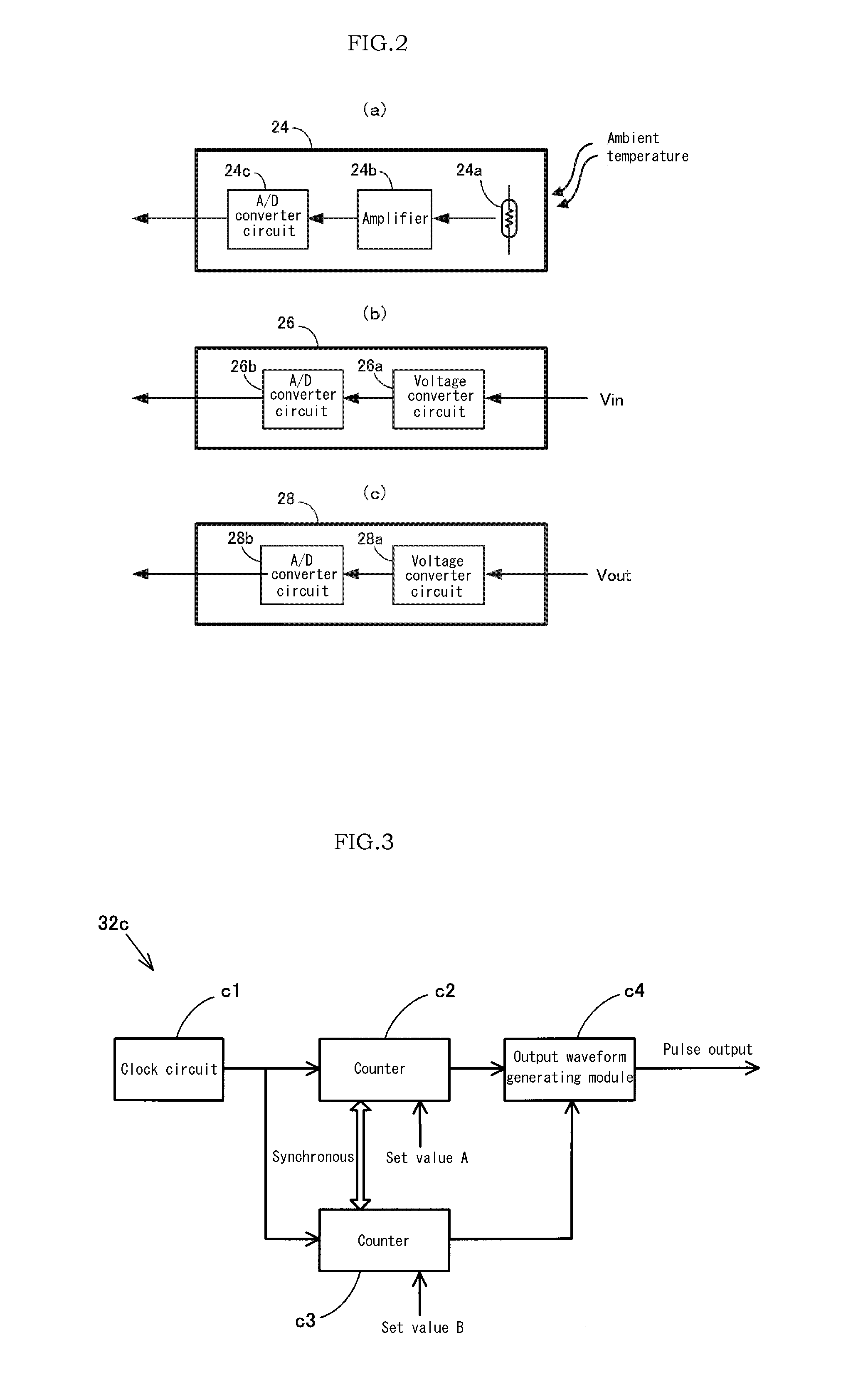
[0057]Hereafter, a description will be given, based on FIGS. 1 to 6, of a switching power source device of the invention. Firstly, a description will be given of an outline, based on the overall circuit diagram shown in FIG. 1. A switching power source device 10 includes an inverter circuit 12 to which a direct current input power source Ein is connected, and which generates an alternating current voltage V2 in accordance with an on-off operation of a switching element TR1, and a rectification and smoothing circuit 14 which rectifies and smoothes the alternating current voltage V2, generating an output voltage Vout, and an output voltage Vout terminal is connected to a load 22. The output voltage Vout is connected to an error amplification circuit 16 configured of an inverting amplifier which outputs an output voltage control signal V(vol), wherein a difference between the output voltage Vout and a predetermined reference voltage Vref is amplified. Furthermore, the switching power s...
second embodiment
[0091]Next, a description will be given, based on FIGS. 7 to 9, of the switching power source device of the invention. Configurations identical to those of the heretofore described switching power source device 10 will be given identical reference numerals and characters, and a description will be omitted. Firstly, a description will be given of an outline, based on the overall circuit diagram of FIG. 7. A switching power source device 50 includes an inverter circuit 12 to which a direct current input power source Ein is connected, and which generates an alternating current voltage V2 in accordance with an on-off operation of a switching element TR1, and a rectification and smoothing circuit 14 which rectifies and smoothes the alternating current voltage V2, obtaining an output voltage Vout, and an output voltage Vout terminal is connected to a load 22. The output voltage Vout is connected to an error amplification circuit 16 configured of an inverting amplifier which outputs an out...
fifth embodiment
[0124]Next, a description will be given, based on FIG. 12, of a fifth embodiment, which is a modification example of the drive pulse generating circuit 18 of the switching power source device of the invention. In a drive pulse generating circuit 62 of the embodiment, as the charging resistor R11 of a sawtooth wave generating circuit 62b is connected to the input voltage Vin, the gradient at which the sawtooth wave voltage V(osc) rises changes in proportion to the input voltage. Because of this, a feed forward control according to the fluctuation of the input voltage is added to the feedback control of the output voltage, and a high-speed responsiveness of an output voltage stabilizing control increases.
[0125]Furthermore, a voltage generating element Rb, at which a voltage proportionate to the input voltage is generated, is inserted at a midpoint of the timer capacitor C11 and charging resistor, and a total value of the voltage generated at the timer capacitor C11 and voltage generat...
PUM
 Abstract
Description
Claims
Application Information


