Transparent Electroconductive Thin Film and Its Production Method

a technology of transparent electroconductive and thin film, which is applied in the direction of conductive layers on insulating supports, coatings, and paper, etc., can solve the problems of limited compatibility between the electroconductivity and light transmittance of thin films, the sense of crisis is increasing, and the indium cost is increasing, so as to achieve high electroconductivity and light transmittance good, high electroconductivity, and high electroconductivity

Active Publication Date: 2010-09-02
JAPAN SCI & TECH CORP
View PDF4 Cites 5 Cited by
  • Summary
  • Abstract
  • Description
  • Claims
  • Application Information

AI Technical Summary

Benefits of technology

[0022]In the production method of the invention, an amine is used as the dispersant, and therefore bundles of single-walled carbon nanotubes can be unbundled and dispersed; and therefore, the resulting dispersion may be applied onto a substrate for film formation to form thereon a thin film of high electroconductivity, and in addition, since m-SWNTs are concentrated through centrifugation or filtration to give the dispersion rich in m-SWNTs, the electroconductivity of the thin film can be greatly increased even though the amount of the single-walled carbon nanotubes to be used is reduced, and a thin film satisfying both high electroconductivity and good light transmittance can be produced. Concretely, for example, the surface resistivity of the thin film can be increased 50 times as compared with that in a case where m-SWNTs are not concentrated.
[0023]In addition, use of an organic polymer as a dispersant or a binder is not indispensable, but an amine having a low boiling point is used as the dispersant; and therefore the operation of dispersing single-walled carbon nanotubes, concentrating m-SWNTs and film formation can be attained in a series of one-process steps in a simplified manner. Since an amine having a low boiling point is used as the dispersant, the amine can be readily removed from the formed thin film through heating, washing or the like after the dispersion is applied onto the substrate; and therefore the dispersant to be an impurity that may bring about reduction in the electroconductivity of the formed film may be readily removed, and a thin film of high electroconductivity can be produced in a simplified manner. Further, since the dispersion and the concentration of single-walled carbon nanotubes with an amine are not accompanied by chemical reaction, the electroconductivity of m-SWNTs is not lowered.
[0024]Since an amine having a low boiling point is used, the degree of concentration of m-SWNTs in the dispersion can be readily controlled by varying the type and the concentration of the amine, the condition in centrifugation, etc.; and as a result, the electroconductivity of the formed thin film can be readily controlled within a broad range of from low electroconductivity to high electroconductivity.
[0025]The transparent electroconductive thin film of the invention is produced by applying onto a substrate single-walled carbon nanotubes prepared by concentrating m-SWNTs by the use of an amine as the dispersant but not substantially containing a polymer such as a polymer dispersant, a binder or the like; and therefore, the electroconductivity of the formed thin film can be greatly increased even though the amount of the single-walled carbon nanotubes to be used is reduced, and the thin film may have high electroconductivity and light transmittance.

Problems solved by technology

However, indium that is the main ingredient of ITO is a rare metal and the exhaustion of indium resources is a serious problem; and the sense of crisis about it is increasing and the indium cost is increasing.
Accordingly, the compatibility between the electroconductivity and the light transmittance of thin films is limited.
In such thin films, the polymer dispersant remains, and therefore, some limitations are given to the compatibility between the electroconductivity and the light transmittance of the thin films and to the process of forming the thin films.

Method used


Image

  • Transparent Electroconductive Thin Film and Its Production Method
  • Transparent Electroconductive Thin Film and Its Production Method
  • Transparent Electroconductive Thin Film and Its Production Method

Examples


example 1

[0067]4 mg of single-walled carbon nanotubes of m-SWNTs and s-SWNTs mixed as bundles (HiPco Tube, by Carbon Nanotechnologies, Inc.) were added to a 5 M propylamine solution (solvent: tetrahydrofuran) and then ultrasonically processed at 5 to 10° C. for 2 hours to thereby uniformly disperse the single-walled carbon nanotubes. Next, this was centrifuged at 45,620 G for 12 hours to prepare a dispersion (hereinafter referred to as “dispersion 1”).

[0068]On the other hand, 4 mg of the single-walled carbon nanotubes as above were added to a 1 M propylamine solution (solvent: tetrahydrofuran) and then ultrasonically processed at 5 to 10° C. for 2 hours to thereby uniformly disperse the single-walled carbon nanotubes. Next, this was centrifuged at 14,000 G for 1 hour to prepare a dispersion (hereinafter referred to as “dispersion 2”).

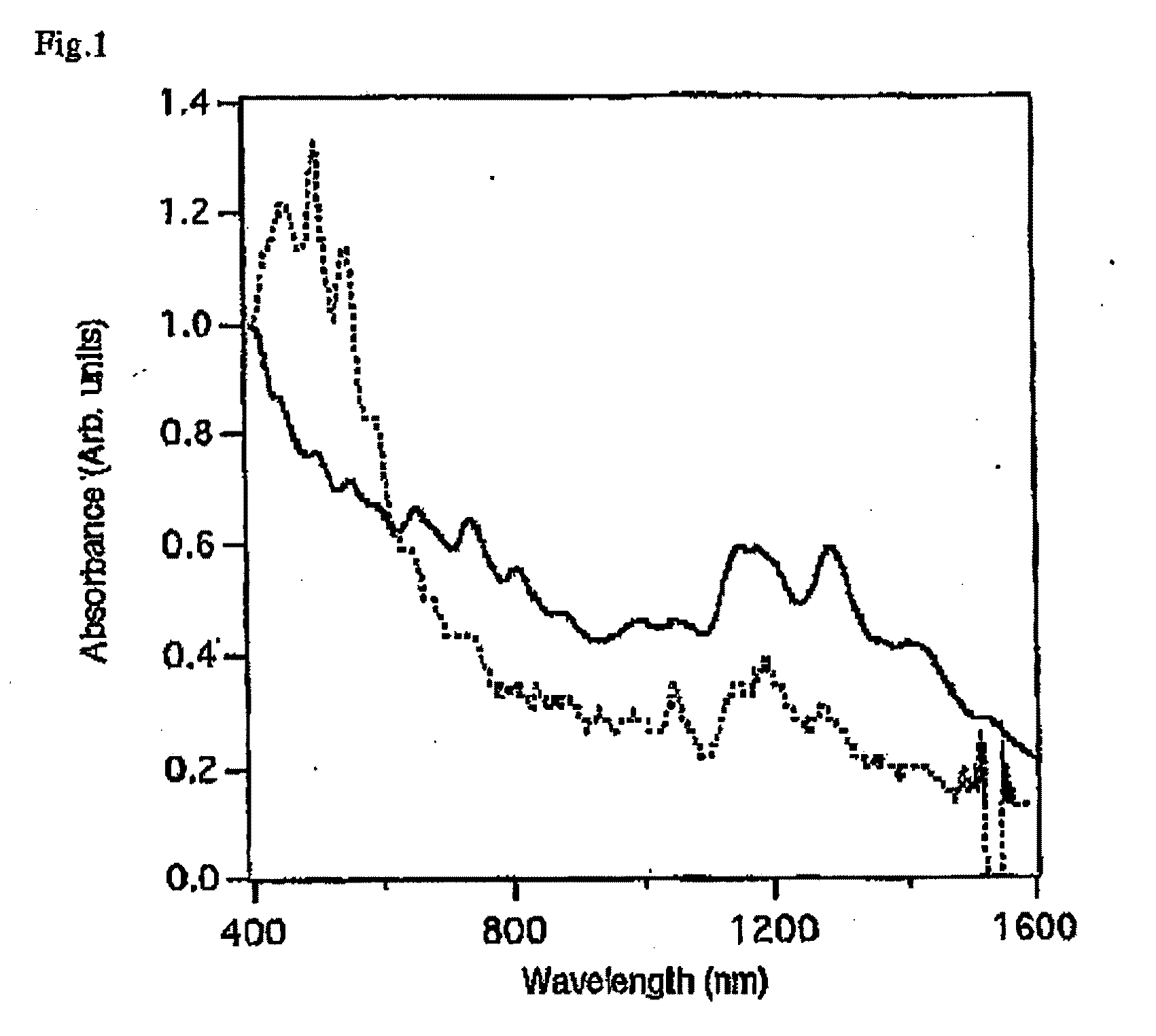
[0069]The single-walled carbon nanotubes in these dispersions 1 and 2 were analyzed through spectrometry. FIG. 1 shows absorption spectra in a wavelength range ...

example 2

[0081]Using an air brush, the dispersion 1 produced in Example 1 was uniformly applied onto the surface of a commercially-available quartz glass sheet having a thickness of 2 mm (transmittance: 93.3%) put on a hot plate at about 85° C., and the solvent tetrahydrofuran and the dispersant propylamine were removed through evaporation by the heat of the hot plate. Next, the thin film was washed with methanol to remove the amine residue, thereby giving a single-walled carbon nanotube thin film-coated quartz glass sheet.

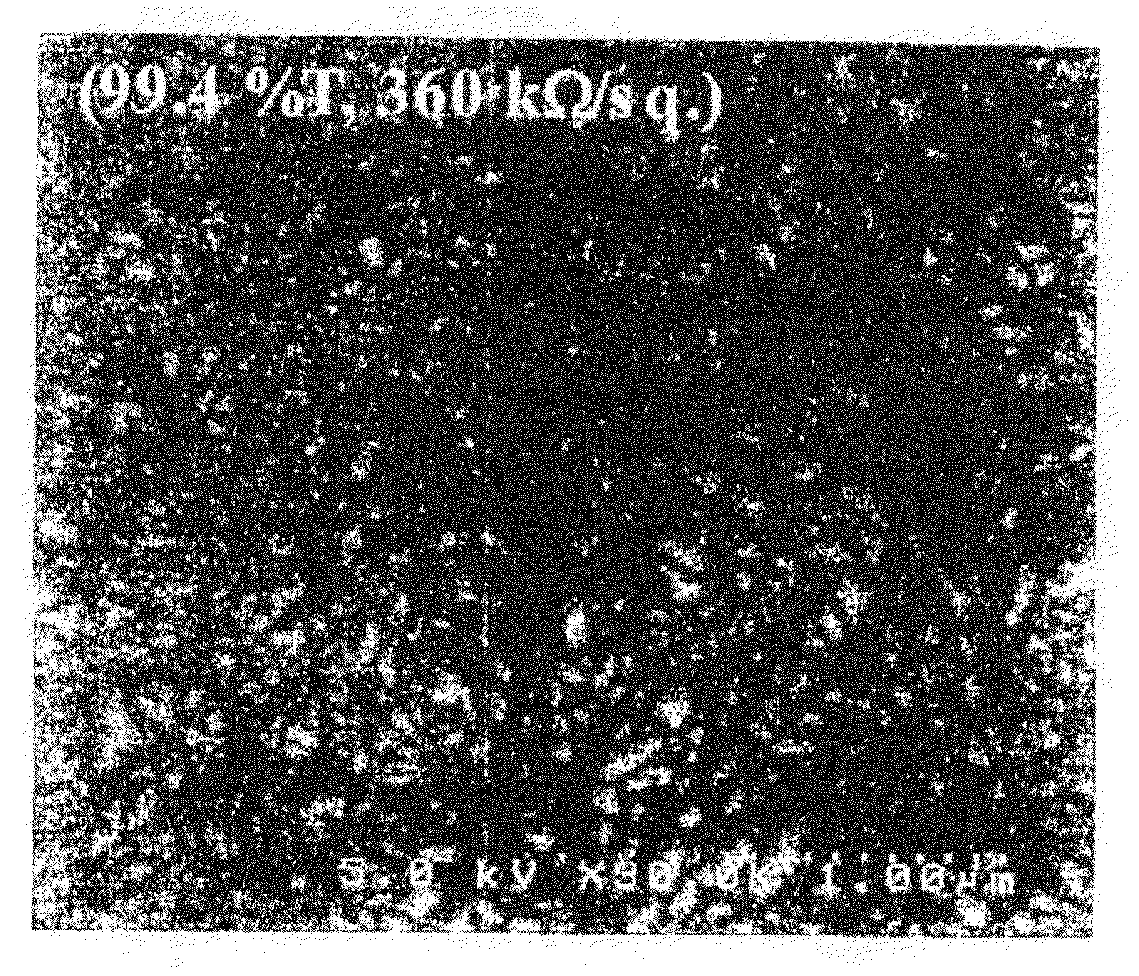
[0082]The thickness of the single-walled carbon nanotube thin film was 28 nm, as measured with a surface profile analyzer. The single-walled carbon nanotube thin film was observed with a scanning electronic microscope and an atomic force microscope, which confirmed the absence of aggregates of single-walled carbon nanotubes but the presence of a large number of single-walled carbon nanotubes individually separated and uniformly dispersed in the film as kept in contact with...

example 3

[0088]Using the dispersions 1 and 2 in Example 1 and in the same manner as in Example 1, plural single-walled carbon nanotube thin films each having a different thickness were formed on the surface of a PET sheet, for which, however, the spraying amount through the air brush was controlled.

[0089]The relationship between the light transmittance and the surface resistivity of these single-walled carbon nanotube thin films are shown in FIG. 3, FIG. 4 and Table 1.

TABLE 1TransmittanceResistivity(after treatment(after treatmentNo. NTsCondition for SeparationSubstrateTransmittanceaResistivitybwith HCl)with HCl)1Dispersion 15 M PropylaminePET99.43600002Dispersion 15 M PropylaminePET98.7240003Dispersion 1b5 M PropylaminePET97.190004Dispersion 1b5 M PropylaminePET96.1480096.436005Dispersion 15 M PropylaminePET81.469082.13306Dispersion 15 M PropylamineQuartz80.78007Dispersion 21 M PropylaminePET98.811900008Dispersion 2c1 M PropylaminePET98.62150009Dispersion 2c1 M PropylaminePET90.23500090.610...


PUM

PropertyMeasurementUnit
boiling pointaaaaaaaaaa
transmittanceaaaaaaaaaa

Abstract

Provided are a transparent electroconductive thin film of single-walled carbon nanotubes and its production method capable of further enhancing the electroconductivity and the light transmittance of the film and capable of simplifying the thin film formation process. The method comprises: dispersing single-walled carbon nanotubes of mixed metallic single-walled carbon nanotubes (m-SWNTs) and semiconductor single-walled carbon nanotubes (s-SWNTs) in an amine solution containing an amine having a boiling point of from 20 to 400° C. as a dispersant; centrifuging or filtering the resulting dispersion to concentrate m-SWNTs, thereby giving a dispersion rich in m-SWNTs; and applying the resulting dispersion rich in m-SWNTs onto a substrate to form a thin film thereon.

Description

TECHNICAL FIELD[0001]The present invention relates to a transparent electroconductive thin film and its production method.BACKGROUND ART[0002]ITO (indium tin oxide) is a compound produced by adding a few % of tin oxide (SnO2) to indium oxide (In2O3); and since it is electroconductive and is highly transparent as having a visible light transmittance of about 90% or so, it is used as an electrode mainly for flat panel displays (FPD); and with the recent increase in the shipment of FPD, the demand for ITO transparent electroconductive thin films is expanding.[0003]However, indium that is the main ingredient of ITO is a rare metal and the exhaustion of indium resources is a serious problem; and the sense of crisis about it is increasing and the indium cost is increasing.[0004]Accordingly, methods of collecting ITO wastes for recycling indium have been proposed, and further, trials of increasing the collection rate have been tried; however, as a radical resolution, development of materia...

Claims


Application Information

Patent Timeline
Patent Type & Authority Applications(United States)
IPC IPC(8): C01B31/30B05D5/12
CPCH01B1/24H01B1/04H01B5/14H01B13/00
Inventor MAEDA, YUTAKAAKASAKA, TAKESHI
Owner JAPAN SCI & TECH CORP
Why Eureka
Try Eureka