Magneto-resistive effect element provided with GaN spacer layer

a technology of magnetoresistive effect and spacer layer, which is applied in the direction of maintaining head carrier alignment, nanoinformatics, instruments, etc., can solve the problems of limited increase of resistance change amount and output, and the technology mentioned above is not suitable in view of reliability, and achieves high resistance spacer layer, simple structure, and high mr ratio

Active Publication Date: 2010-09-16
TDK CORPARATION
View PDF10 Cites 13 Cited by
  • Summary
  • Abstract
  • Description
  • Claims
  • Application Information

AI Technical Summary

Benefits of technology

[0011]The object of the present invention is to provide an MR element that has a high MR ratio by obtaining a high resistance spacer layer with a sim...

Problems solved by technology

However, a conventional CPP-GMR element with a spacer layer that is made of Cu has a limited increase of resistance change amount and output, which is obtained as a result of the increase o...

Method used


Image

  • Magneto-resistive effect element provided with GaN spacer layer
  • Magneto-resistive effect element provided with GaN spacer layer
  • Magneto-resistive effect element provided with GaN spacer layer

Examples


first embodiment

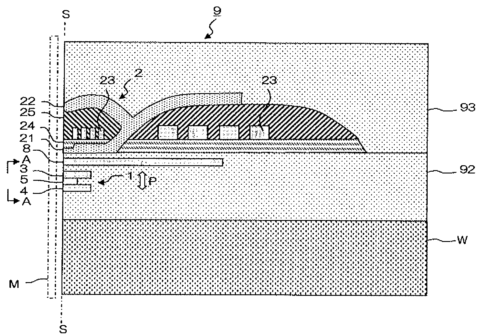
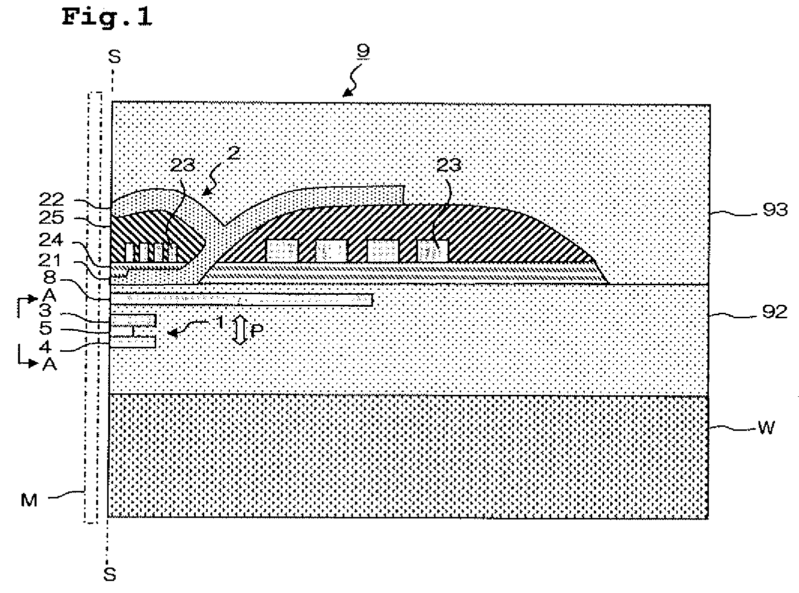
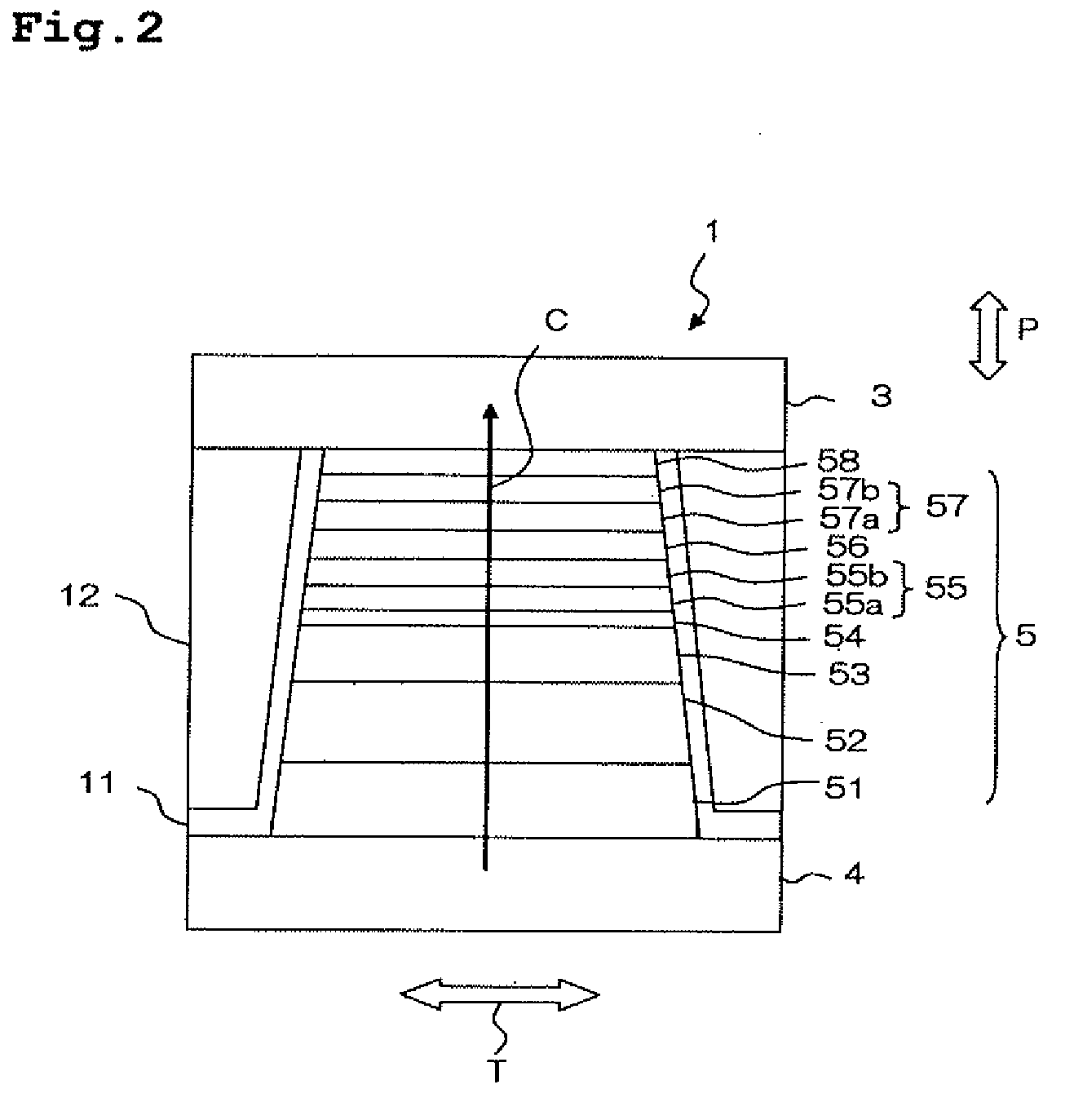
[0033]FIG. 1 is a sectional view of a main part of such the thin film magnetic head. A thin film magnetic head 9 includes a reproducing head 1 and a recording head 2, which are formed on a substrate W. FIG. 2 is a side view of the reproducing head seen from the A-A direction in FIG. 1, namely the ABS S. The ABS S is defined as a side opposite to a recording medium M of the thin film magnetic head 9. First, as shown in FIG. 2, an explanation of the structure of the reproducing head 1 will be given.

[0034]The reproducing head 1 includes an MR element 5 made with several layers, an upper shield electrode layer 3 and a lower shield electrode layer 4 that sandwich the MR element 5 in a film surface orthogonal direction (lamination direction) P. The edge portion of the MR element 5 is, as shown in FIG. 1, exposed at the ABS S. Because of the applied voltage between the upper shield electrode layer 3 and the lower shield electrode layer 4, a sense current C flows in a film surface orthogona...

second embodiment

[0055]FIG. 3 is a perspective view of a main part of a reproducing head 1a seen from the ABS of the thin film magnetic head according to the present embodiment. FIG. 4 is a partial enlarged perspective view of FIG. 3. The thin film magnetic head according to the present embodiment has the same structure of the first embodiment shown in FIG. 1 except for the structure of the reproducing head 1a. The reproducing head 1 includes an MR element 7 made with several layers that are laminated, and an upper shield electrode layer 3a and a lower shield electrode layer 4a, which sandwich the MR element 7 in a film surface orthogonal direction (lamination direction) P in the manner of the first embodiment. Table 3 shows an example of layer configurations of the MR element 7. Table 3 shows laminated layers from an exchange coupling transmitting layer 71, which contacts the lower shield electrode layer 4a, to an exchange coupling transmitting layer 79, which contacts the upper shield electrode la...


PUM


Abstract

A magneto-resistive effect (MR) element includes a first magnetic layer and a second magnetic layer in which a relative angle of magnetization directions of the first and second magnetic layers changes according to an external magnetic field; and a spacer layer that is provided between the first magnetic layer and the second magnetic layer. The spacer layer contains gallium nitride (GaN) as a main component. A thin film magnetic head according to one embodiment of the present invention is provided with the following structures: an MR element mentioned above that has a first magnetic layer and a second magnetic layer, as free layers, in which the magnetization direction in the two layers changes according to the external magnetic field; a bias magnetic field application layer that applies a bias magnetic field to the first and second magnetic layers in an orthogonal direction to an air bearing surface (ABS); the bias magnetic field application layer is formed in a rear side of the MR element seen from the ABS; and a sense current flows in an orthogonal direction to a layer surface of the MR element.

Description

BACKGROUND OF THE INVENTION[0001]1. Field of the Invention[0002]The present invention relates to magneto-resistive effect elements (MR elements). Specifically, the present invention relates to the structure of a spacer layer.[0003]2. Description of the Related Art[0004]A thin film magnetic head that uses a giant magneto-resistive effect element (GMR element) as a reproducing head has been developed to correspond with the high recording density of a hard disk drive (HDD). Especially, a GMR element using a spin valve (SV) layer contributes to providing high sensitively thin film magnetic heads since a GMR element has a large resistance change ratio (MR ratio) to a sense current that flows in an element to read records written in a recording medium.[0005]A current in plane (CIP)-GMR element in which a sense current flows in a parallel direction to a layer surface formed for the element was a main element among MR elements using a SV layer. However, recently a thin film magnetic head us...

Claims


Application Information

Patent Timeline
IPC IPC(8): G11B5/60G11B5/127G11B5/48
CPCB82Y10/00B82Y25/00G01R33/093H01L43/10G11B5/3906G11B2005/3996H01L43/08G01R33/098H10N50/85H10N50/10
Inventor HARA, SHINJITSUCHIYA, YOSHIHIROCHOU, TSUTOMUMATSUZAWA, HIRONOBU
Owner TDK CORPARATION
Why Eureka
Try Eureka