Magnetoresistive element, and magnetic random access memory

a magnetic random access memory and magnetoresistive element technology, applied in the field of magnetoresistive element and magnetic random access memory, can solve the problems of increasing the write current, increasing the power consumption of writing, and poor competitiveness compared with other random access memory, so as to reduce the write current, the effect of reducing the write current and high thermal stability

Active Publication Date: 2010-09-23
NEC CORP
View PDF2 Cites 11 Cited by
  • Summary
  • Abstract
  • Description
  • Claims
  • Application Information

AI Technical Summary

Benefits of technology

[0012]In the magnetoresistive element of the present invention, in which the first magnetization free layer in which the current-driven domain wall motion occurs is made of the material having a magnetic anisotropy in the film thickness direction, the domain wall can be driven even with a small current density, due to the spin torque term in an LLG equation in view of the spin-polarized current. Here, the domain wall motion can be caused with substantially no influence by a de-pin magnetic field, and thus the current necessary for writing is decreased in the magnetoresistive element of the present invention, while the high thermal stability and the external disturbance magnetic field resistance are kept. In addition, the data stored as the direction of the magnetization of the magnetization free region in the first magnetization free layer is transmitted to the second magnetization free layer, which has a magnetic anisotropy in the in-plane direction, through the magnetic coupling between the magnetization free region and the second magnetization free layer. This allows reading by using the magnetic tunnel junction formed with the first magnetization fixed layer and the second magnetization free layer, which have magnetization components in the in-plane longitudinal direction. Thus, a high magnetoresistance ratio is obtained by properly selecting the materials of the second magnetization free layer, the nonmagnetic layer and the first magnetization fixed layer.

Problems solved by technology

When the write current is large, the chip area is inevitably increased and the power consumption necessary for writing is also increased, which causes poor competitiveness compared with other random access memories.
In addition, when the size reduction of memory cells causes a further increase in the write current; this is undesirable from the viewpoint of scaling.
This causes a problem of rewriting durability and reliability.
Also, a current path is commonly used in writing and reading, and this may cause an erroneous writing in reading.
As thus described, there are several obstacles in attaining the practical use of the spin injection magnetization reversal, although the spin injection magnetization reversal is superior in the scaling property.
However, an MRAM that uses the current-driven domain wall motion suffers from a problem that the absolute value of the write current is relatively large.
Also, the reduction in the width of the ferromagnetic film down to 100 nm or less involves the severe difficulty from the viewpoint of the processing technique.
The use of the film made of vertical magnetic anisotropic material in the magnetic recording layer, however, makes it difficult to increase the magnetoresistance ratio (MR ratio), which corresponds to the SN ratio of the reading signal of the MRAM, resulting in a problem that the compatibility with the reading property is difficult.

Method used


Image

  • Magnetoresistive element, and magnetic random access memory
  • Magnetoresistive element, and magnetic random access memory
  • Magnetoresistive element, and magnetic random access memory

Examples


first modification

(First Modification)

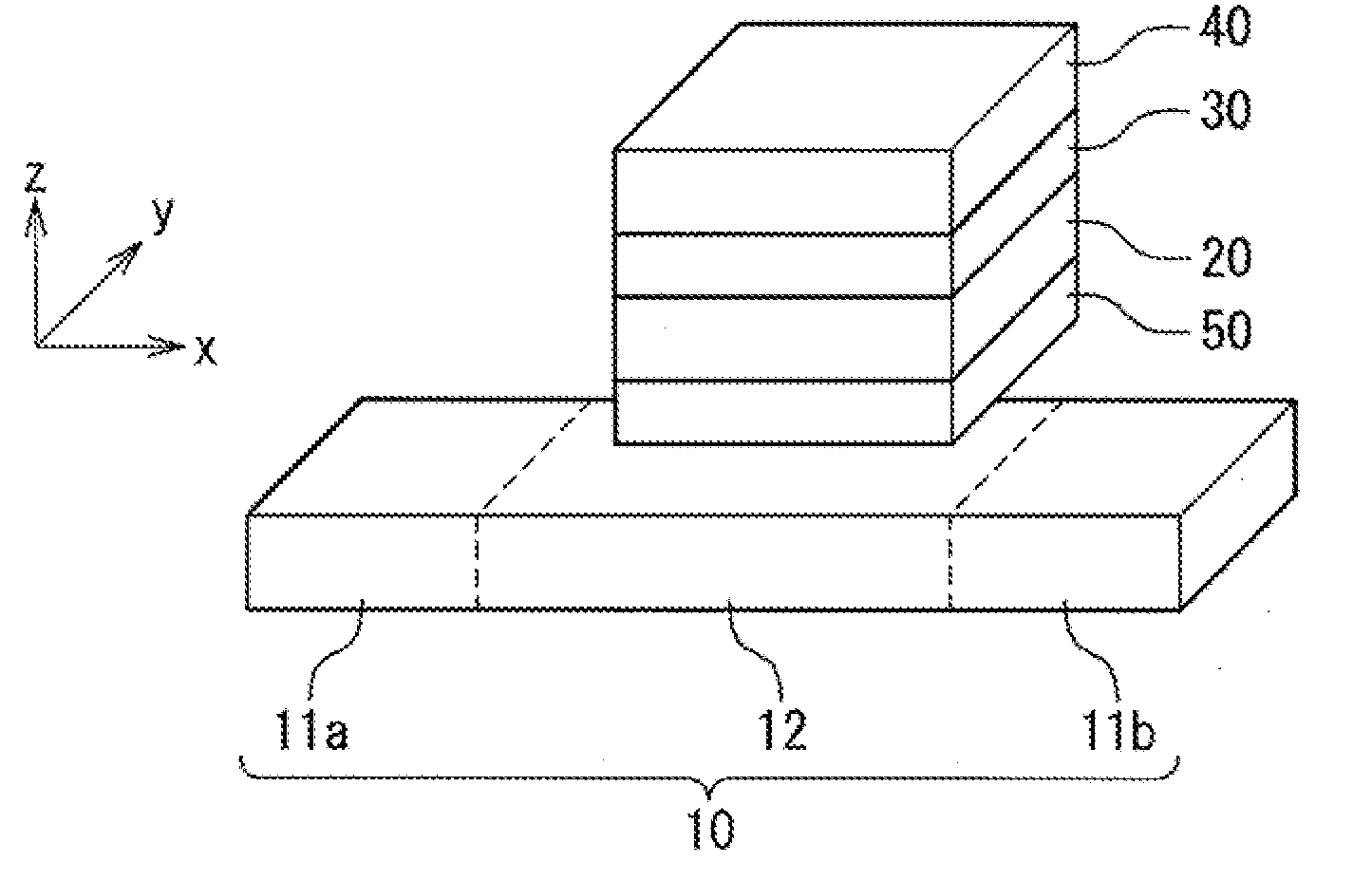
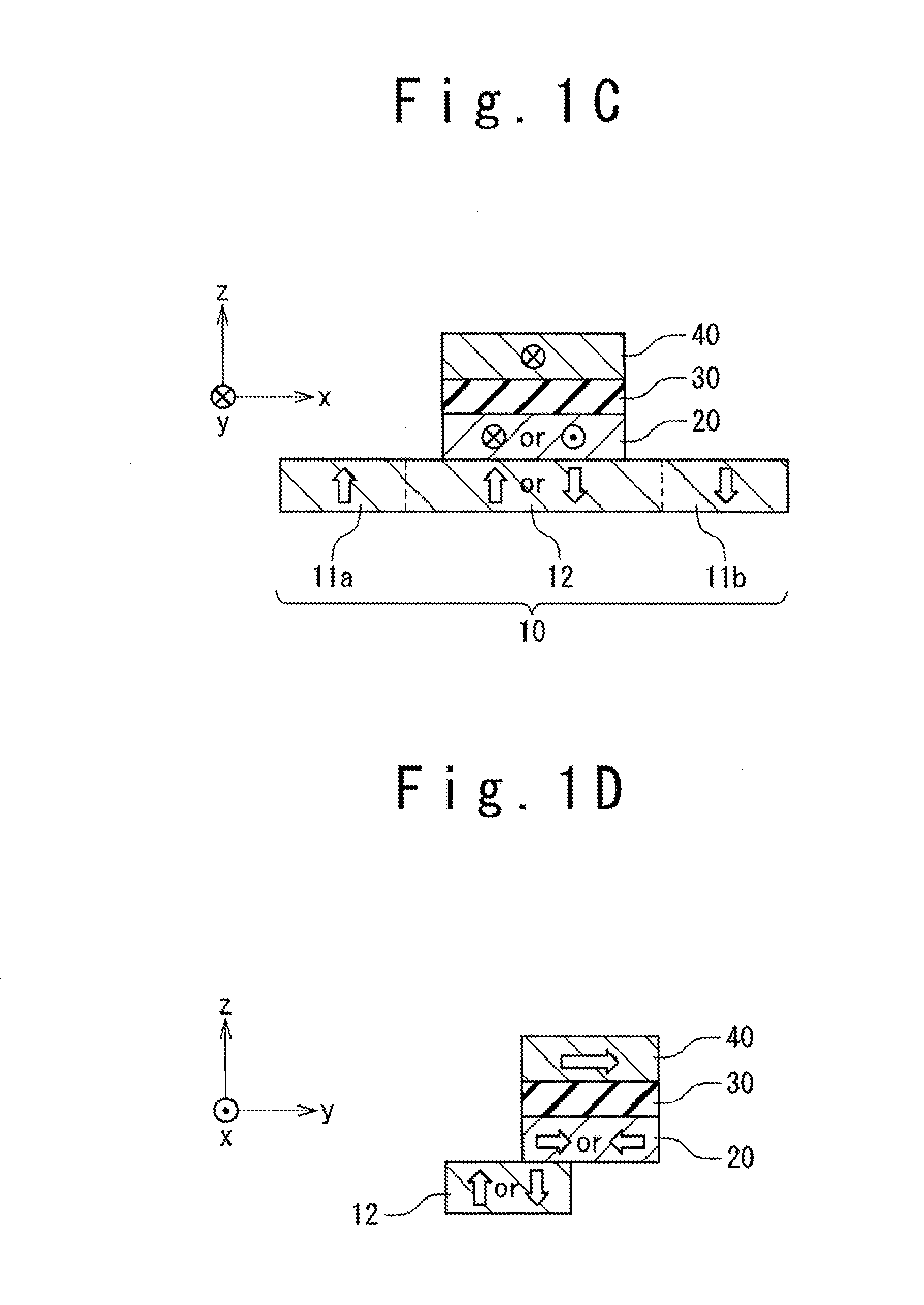
[0110]FIG. 4A to FIG. 4C and FIG. 5A to FIG. 5C schematically show structures of a first modification of the magnetoresistive element of this embodiment. FIG. 4A to FIG. 4C show one implementation of the first modification, and FIG. 5A to 5C show another implementation. Among them, FIG. 4A, FIG. 5A are perspective views, and FIG. 4B, FIG. 5B are x-z sectional views in FIG. 4A, FIG. 5A, and FIG. 4C, FIG. 5C show y-z sectional view in FIG. 4A, FIG. 5A.

[0111]In detail, in the first modification, a conductive layer 50 is formed between the first magnetization free layer 10 and the second magnetization free layer 20. The conductive layer 50 is formed of a conductor. It should be noted that the conductive layer 50 may be magnetic or non-magnetic. When the conductive layer 50 is magnetic, the conductive layer 50 is preferably formed of relatively soft magnetic material. Also, the conductive layer 50 may be configured by the lamination film made of a plurality of materia...

second modification

(Second Modification)

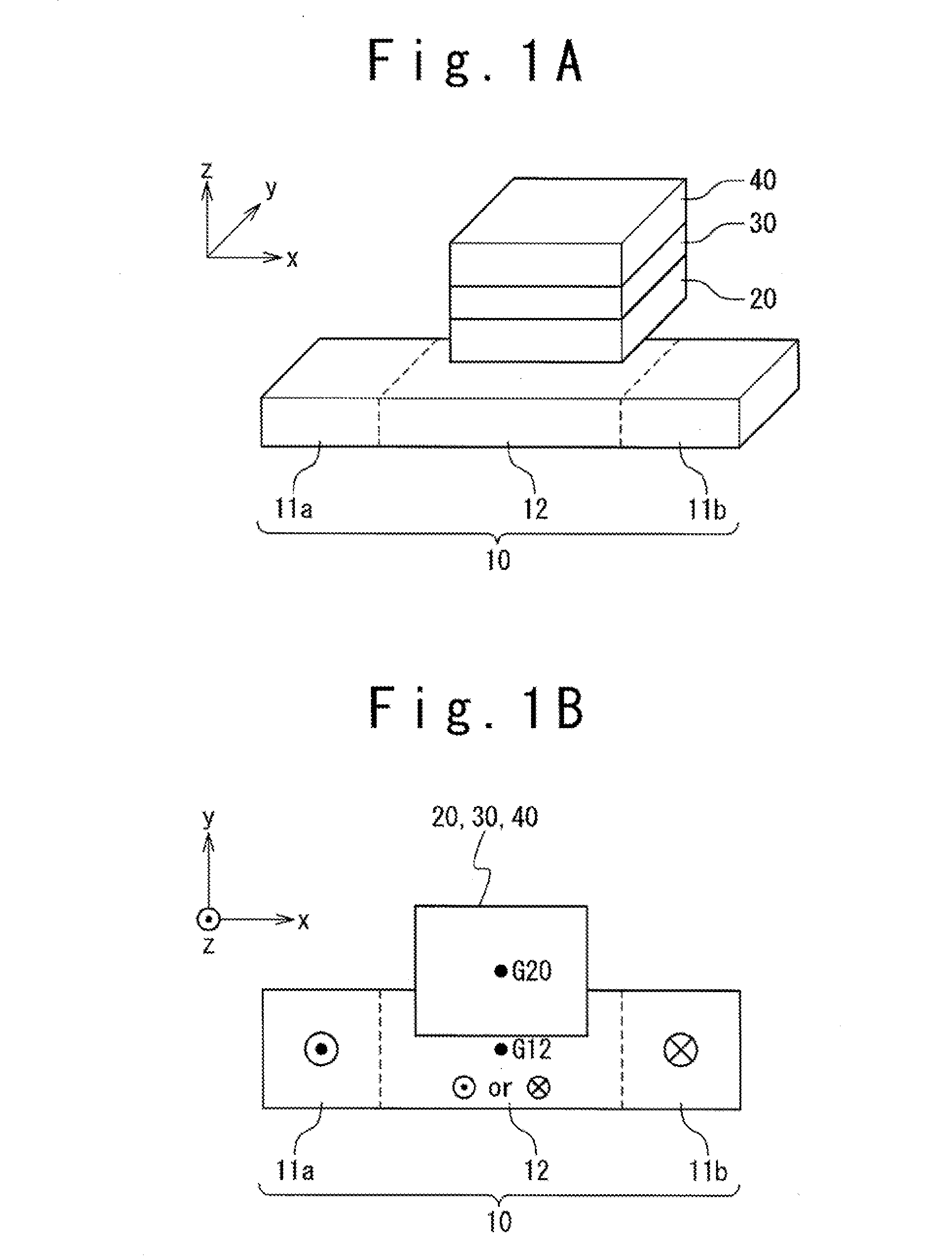
[0115]FIGS. 6A to 6C, FIGS. 7A to 7C, and FIGS. 8A to 8C schematically show structures of the second modification of the magnetoresistive element in this embodiment. The second modification relates to the positional relation between the first magnetization free layer 10 and the second magnetization free layer 20.

[0116]One feature of the magnetoresistive element in this embodiment lies in the arrangement in which the center of mass G20 of the second magnetization free layer 20 is disposed displaced in the in-plane direction (namely, the direction parallel to the x-y plane), with respect to the center of mass G12 of the magnetization free region 12 in the first magnetization free layer 10, and the positional and size relations may be variously changed. Thus, various structures as well as the structures shown in FIG. 1A to FIG. 1D may be used for the magnetoresistive element in this embodiment. FIGS. 6A, 7A and 8A are perspective views of the respective structures,...

third modification

(Third Modification)

[0118]FIGS. 9A to 9C schematically show the structure of the third modification of the magnetoresistive element in this embodiment. The third modification relates to the positional and size relations between the second magnetization free layer 20 and the first magnetization fixed layer 40.

[0119]In the magnetoresistive element in this embodiment, the second magnetization free layer 20 and the first magnetization fixed layer 40 may at least partially overlap with each other in the x-y plane; the positional and size relations are arbitrary. Thus, the structure shown in FIGS. 9A to 9C as well as the structure shown in FIG. 1A to FIG. 1D may be used in the magnetoresistive element in this embodiment. FIG. 9A is the perspective view of the magnetoresistive element in the third modification, FIG. 9B is the x-y plan view, and FIG. 9C is the y-z sectional view. FIGS. 9A to 9C show an example in which the first magnetization fixed layer 40 is formed to overlap with a part ...


PUM


Abstract

A magnetoresistive element is provided with a first magnetization free layer; a second magnetization free layer; a non-magnetic layer disposed adjacent to the second magnetization free layer; and a first magnetization fixed layer disposed adjacent to the second magnetization free layer on an opposite side of the second magnetization free layer. The first magnetization free layer is formed of ferromagnetic material and has a magnetic anisotropy in a thickness direction. On the other hand, the second magnetization free layer and the first magnetization fixed layer are formed of ferromagnetic material and have a magnetic anisotropy in an in-plane direction. The first magnetization free layer includes: a first magnetization fixed region having a fixed magnetization; a second magnetization fixed region having a fixed magnetization; and a magnetization free region connected to the first and second magnetization fixed regions and having a reversible magnetization. The magnetization free region and the second magnetization free layer are magnetically coupled. In addition, the center of mass of the magnetization free region and the center of mass of the second magnetization free layer are displaced in a particular in-plane direction.

Description

TECHNICAL FIELD[0001]The present invention relates to a magnetoresistive element and a magnetic random access memory, and more particularly to a domain wall'motion type magnetoresistive element and magnetic random access memory.BACKGROUND ART[0002]Magnetic random access memories (MRAMs) are expected to be nonvolatile memories which provide a high speed operation and an infinite number of rewritings, and vigorous developments thereof have been carried out. In an MRAM, a magnetoresistive element is integrated within a memory cell, and a data is stored as the orientation of the magnetization of the ferromagnetic layer of the magnetoresistive element. Although several approaches have been proposed as a method of switching the magnetization of the ferromagnetic layer, all of them are common with regard to the use of a current. In putting into the practical use, the reduction of the write current is very important, and there is a requirement lot the reduction down to 0.5 mA or less, prefe...

Claims


Application Information

Patent Timeline
Patent Type & Authority Applications(United States)
IPC IPC(8): H01L29/82
CPCG11C11/16H01L43/08H01L27/228G11C19/0808G11C11/1655G11C11/1659G11C11/161G11C11/1673G11C11/1675G11C11/1657H10B61/22H10N50/10
Inventor FUKAMI, SHUNSUKEISHIWATA, NOBUYUKISUZUKI, TETSUHIRONAGAHARA, KIYOKAZUOHSHIMA, NORIKAZU
Owner NEC CORP
Why Eureka
Try Eureka