Eureka AIR delivers breakthrough ideas for toughest innovation challenges, trusted by R&D personnel around the world.

Electronic circuit board manufacturing method

a manufacturing method and electronic circuit board technology, applied in the direction of superimposed coating process, liquid/solution decomposition chemical coating, resistive material coating, etc., can solve the problems of large amount of waste liquid, cracking or detachment, and time-consuming wiring pattern formation, so as to reduce standing time at room temperature, enhance the cohesiveness and enhance the cohesion of metal colloidal particles

Inactive Publication Date: 2010-09-23
FUJIFILM CORP
View PDF3 Cites 5 Cited by
  • Summary
  • Abstract
  • Description
  • Claims
  • Application Information

AI Technical Summary

Benefits of technology

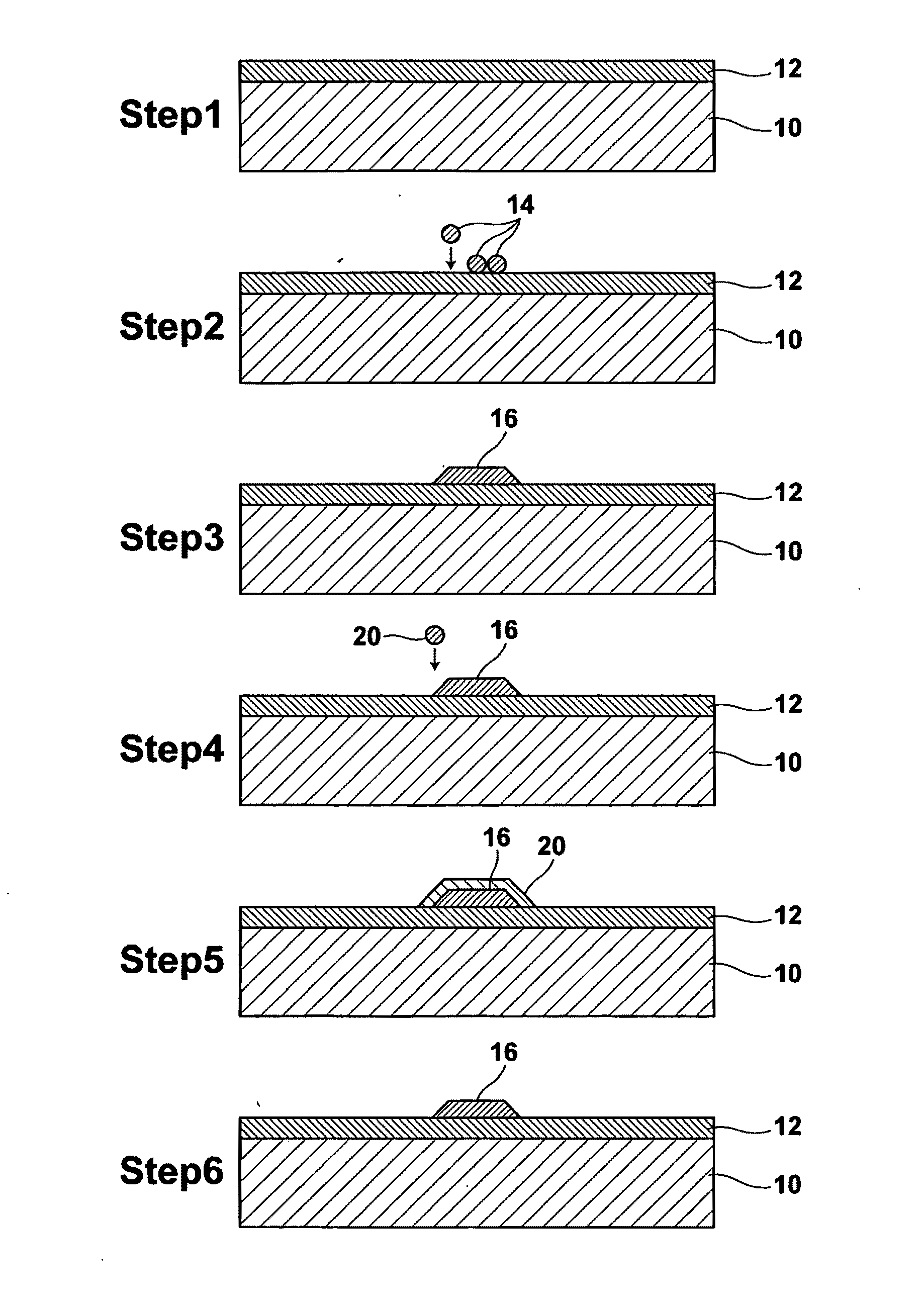
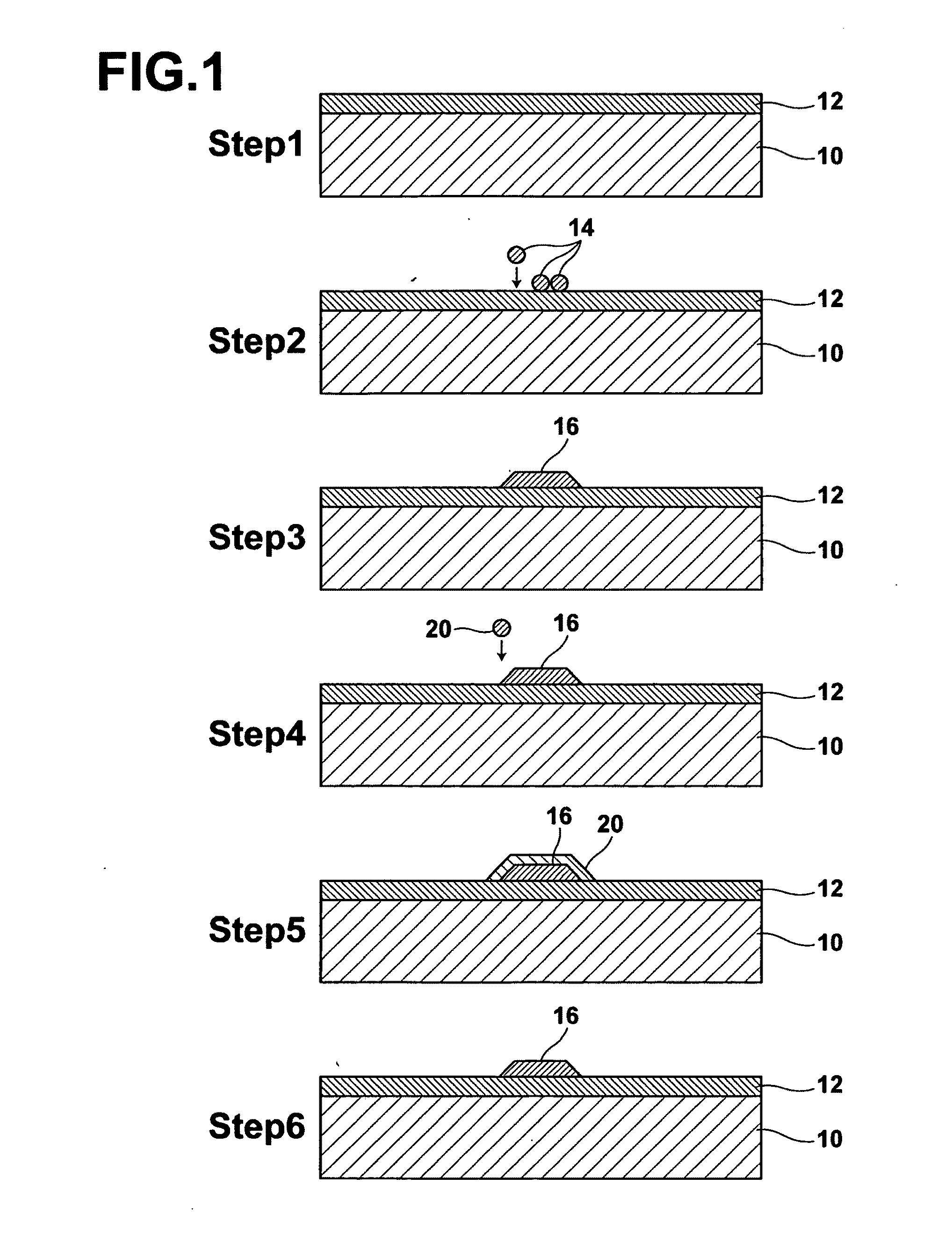
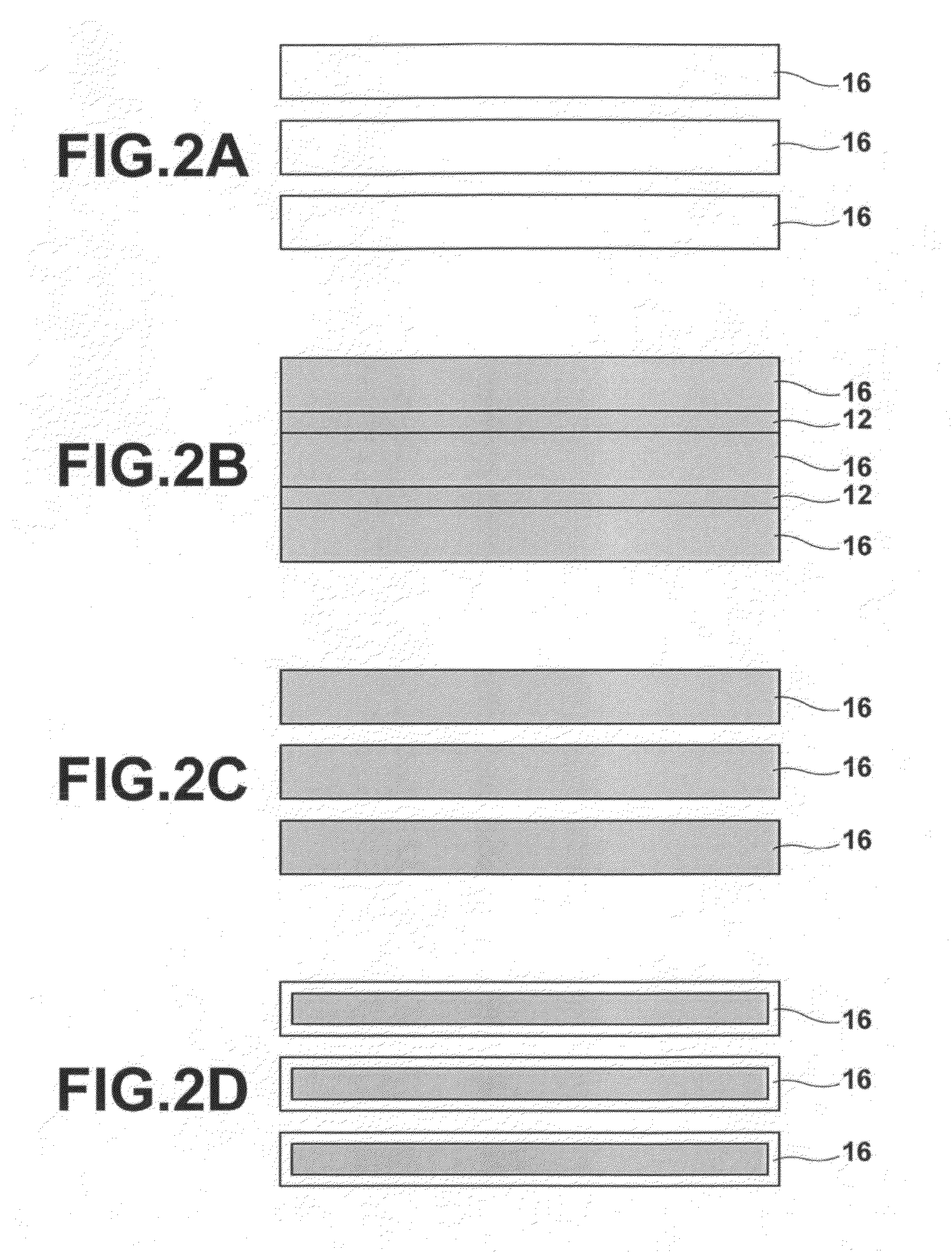
[0046]Consequently, the cohesiveness of the metal colloidal particles in the metal colloid solution is enhanced by simply leaving the solution at room temperature without heating due to the presence of the coagulant solution. Since the cohesiveness of the metal colloidal particles is enhanced, the standing time at room temperature may be reduced, resulting in a reduced manufacturing time. Further, since the cohesiveness of the metal colloidal particles is enhanced, a conductive pattern may be formed without spoiling the conductivity. Still further, any heating equipment is required since heating process is not required, whereby the manufacturing cost may be reduced. Further, the base material needs not to have high heat resistivity, which increases the selection freedom of base material and a general purpose base material may be used. Thus, according to the present invention, electronic circuit boards may be manufactured efficiently at a low cost without increasing the size of the manufacturing facilities.
[0047]In particular, in the second electronic circuit board manufacturing method of the present invention, an entire base material surface application method, such as a bar coating method may be selected as the application method of the coagulant solution. Consequently, the coating process of coagulant solution may be simplified, resulting in a reduced manufacturing cost. Further, the coagulation action is started immediately after the metal colloid solution is applied on the base material, so that the interference between adjacently applied metal colloid solutions during the application of the metal colloid solution may be prevented.
[0048]Further, in the first electronic circuit board manufacturing method of the present invention, the cohesiveness of the metal colloidal particles may be further enhanced by applying the coagulant solution in an amount greater than an application amount of the metal colloid solution and whereby the standing time at room temperature may further be reduced.
[0049]Still further, in the first electronic circuit board manufacturing method of the present invention, the consumed amount of coagulant solution may be reduced by limiting the application area of the coagulant solution smaller than the application area of the metal colloid solution. Further, this will result in that the coagulant solution is applied concentratingly only on a required portion, so that the coagulation of the metal colloidal particles may be efficiently enhanced, which may further reduce the standing time at room temperature. Still further, the conductive pattern formed with the metal colloid solution may be prevented from wet-spreading, since the coagulant solution is applied only on a required portion.
[0050]Further, in the third electronic circuit board manufacturing method of the present invention, a reception layer-equipped base material is used. Still further, in the first and second electronic circuit board manufacturing methods of the present invention, the base material may be turned into a reception layer-equipped base material having a porous reception layer formed on a surface thereof. This will result in that the metal colloid solution is applied on the reception layer, so that the adhesion between the base material and conductive pattern formed with the metal colloid solution may be increased. Consequently, even when the solvent of the metal colloid solution and the coagulant solution are applied on top of each other, the shape of the conductive pattern formed with the metal colloid solution is ensured. This allows, therefore, the application amount of the coagulant solution to be increased, whereby the cohesiveness of the metal colloidal fine particles may further be enhanced. Further, the conductive pattern formed is free from defects as wiring, such as a short circuit or an open circuit.

Problems solved by technology

Further, the method also requires resist exposure and development processing for forming a resist pattern aside from the etching for removing an unnecessary portion of wiring metal.
Consequently, formation of a wiring pattern takes time and cost.
The method also poses a problem of treating a large amount of waste liquid due to the exposure and development processing.
Still further, cracking or detachment may occur in the pattern or otherwise the base material itself is damaged if the type and amount of solvent used, and immersion time are not selected appropriately.
Consequently, base materials on which a wiring pattern can be formed are limited to heat resistive materials.
In addition, high running and manufacturing costs are required with an inevitable large equipment size for high temperature processing.
In the method describe in Japanese Unexamined Patent Publication No. 2008-066568, if the first and second inks are not appropriately brought into contact, the two types of inks are not mixed together and a desired electrical property may not be obtained.
Consequently, ink drop control becomes complicated, which makes it difficult to form a complicated conductive pattern.

Method used


Image

  • Electronic circuit board manufacturing method
  • Electronic circuit board manufacturing method
  • Electronic circuit board manufacturing method

Examples


examples

[0244]Electronic circuit boards were produced as Examples of the present invention and Examples were evaluated, the results of which will now be described.

examples 1 , 2

Examples 1, 2

[0245]For examples 1, 2, glass was used as base material 10. As coagulant solution 20, an aqueous solution of Alphaine 83 (aluminum chloride), manufactured by Taimei Chemicals Co., Ltd., diluted to a concentration of 2% with ion-exchange water was used. As the solvent of metal colloid solution 14, NPS-J, manufactured by Harima Chemicals, Inc., was used (for Example 1, the solvent used is tetradecane) and AGIN-W4A, manufactured by Sumitomo Electric Industries Ltd., was used (for Example 2).

[0246]Coagulant solution 20 was applied over a surface of base material 10 by a bar coating method, then the applied solution was dried at 70° C. for 5 minutes, and a conductive pattern was formed with metal colloid solution 14. Then, 6 days after the formation of the conductive pattern, the volume resistivity of the conductive pattern was measured using Loresta-GP manufactured by Mitsubishi Chemical Corporation. For each of Examples 3 to 6 to be described hereinafter, the volume resis...

example 3

[0247]As base material 10 having reception layer 12 formed thereon, an inkjet receiver paper (Kassai, “Photofinishing” Value) manufactured by FUJIFILM Corporation was used. As coagulant solution 20, an aqueous solution of Alphaine 83 (aluminum chloride), manufactured by Taimei Chemicals Co., Ltd., diluted to a concentration of 2% with ion-exchange water was used. As the solvent of metal colloid solution 14, AGIN-W4A, manufactured by Sumitomo Electric Industries Ltd., was used.


PUM

PropertyMeasurementUnit
widthaaaaaaaaaa
widthaaaaaaaaaa
widthaaaaaaaaaa

Abstract

An electronic circuit board is formed by a pattern forming step for forming a conductive pattern of an electronic circuit board by applying a metal colloid solution on a base material by an inkjet method and a coagulant application step for applying a coagulant solution at least on the conductive pattern by a deposition method.

Description

BACKGROUND OF THE INVENTION[0001]1. Field of the Invention[0002]The present invention relates to an electronic circuit board manufacturing method, and more particularly to an electronic circuit board manufacturing method for forming a wiring of an electronic circuit board.[0003]2. Description of the Related Art[0004]Heretofore, as methods for forming a pattern of a wiring portion (conductor portion) of an electronic circuit board (printed wiring board), subtractive method, semi-additive method, and additive method are known.[0005]The subtractive method is a method for forming a pattern of conductor portion (wiring pattern) by removing an unnecessary portion of a metal layer formed on a base material while leaving a necessary portion. In contrast, the semi-additive or additive method is a method for additively forming a pattern of conductor portion on a base material. In each case, the pattern of conductor portion is formed based on a photolithography technology.[0006]The subtractive...

Claims


Application Information

Patent Timeline
Patent Type & Authority Applications(United States)
IPC IPC(8): B05D5/12
CPCH05K3/1208H05K3/125H05K2203/125H05K2201/0116H05K2203/122H05K3/1283
Inventor YOSHIDA, JUNICHIINOUE, SEIICHIONO, WATARUKAWAKAMI, HIROSHI
Owner FUJIFILM CORP
Why Eureka
Eureka Blog
Learn More