METHOD FOR PRODUCING SINGLE CRYSTAL SiC SUBSTRATE AND SINGLE CRYSTAL SiC SUBSTRATE PRODUCED BY THE SAME

a technology of single crystal sic substrate, which is applied in the direction of crystal growth process, polycrystalline material growth, chemistry apparatus and processes, etc., can solve the problems of high price of sic single crystal itself, small area, and high cost of obtainable sic single crystal, and suppress the warp of the entire substrate. , the crystallinity of the sic layer is formed, and the softening point is lower

Active Publication Date: 2010-10-07
PUBLIC UNIVERSITY CORPORATION OSAKA CITY UNIVERSITY +1
View PDF2 Cites 1 Cited by
  • Summary
  • Abstract
  • Description
  • Claims
  • Application Information

AI Technical Summary

Benefits of technology

[0013]That is, the method for producing the single crystal SiC substrate according to a first aspect of the invention includes the carbonization process in which an embedded oxide layer in an SOI substrate is converted into an embedded glass layer having a lower softening point, and thereafter, the resulting substrate is heated in an atmosphere of hydrocarbon-based gas and cooled. Therefore, even if a difference of shrinkage ratios is generated between the SiC layer and the Si base material layer formed in the carbonization process, the embedded glass layer between the SiC layer and the Si base material layer is transformed to generate a slip between the Si base material layer and the SiC layer, greatly suppressing the warp of the entire substrate.
[0014]In the method for producing a single crystal SiC substrate according to the first aspect of the invention, if an introduction amount of the P-type ions in the P-type ion introduction step is from 1×10¹⁵ to 5×10¹⁸ ions / cm2, a warp of the substrate can be effectively suppressed with crystallinity of the SiC layer formed being maintained well.
[0015]In the method for producing a single crystal SiC substrate according to the first aspect of the invention, the substrate temperature is 200 to 550° C. in the P-type ion introduction step, the crystallinity of the surface Si layer is maintained well and a good SiC layer can be ensured in the carbonization step. In the method for producing a single crystal SiC substrate according to the first aspect of the invention, the P-type ion introduction step is performed by ion implantation, and if an accelerating energy of the P-type ions at which the time is 5 to 30 keV, the ion implantation can be conducted with the crystallinity of the surface Si layer being maintained. As a result, warp of the substrate can be effectively suppressed.
[0016]Further, a method for producing a single crystal SiC substrate according to a second aspect of the invention includes a carbonization process in which the embedded type substrate is formed which has the embedded glass layer lower in the softening point than at least the SiO2 embedded between the Si base material layer and the surface Si layer, and thereafter, the resulting substrate is heated in an atmosphere of hydrocarbon-based gas and cooled. Therefore, even if a difference of shrinkage ratios is generated between the SiC layer and the Si base material layer formed in the carbonization process, the embedded glass layer between the SiC layer and the Si base material layer is transformed to generate a slip between the Si base material layer and the SiC layer, greatly suppressing the warp of the entire substrate.
[0017]Moreover, a single crystal SiC substrate according to the invention includes the embedded glass layer lower in the softening point than at least the SiO2 embedded between the Si base material layer and the surface single crystal Si layer. Therefore, even if the carbonization process is performed in which the resulting substrate is heated in an atmosphere of hydrocarbon-based gas and cooled, the embedded glass layer between the SiC layer and the Si base material layer is transformed to generate a slip between the Si base material layer and the SiC layer, greatly suppressing the warp of the entire substrate.

Problems solved by technology

However, in the above method in which the SiC single crystal is used as starting material, the obtainable SiC single crystal itself is highly expensive and has a small area in fact.
Therefore, it is extremely expensive as a semiconductor device as well, thus, strongly demanded is a technique to provide a single crystal SiC substrate having a large area at low cost.

Method used


Image

  • METHOD FOR PRODUCING SINGLE CRYSTAL SiC SUBSTRATE AND SINGLE CRYSTAL SiC SUBSTRATE PRODUCED BY THE SAME
  • METHOD FOR PRODUCING SINGLE CRYSTAL SiC SUBSTRATE AND SINGLE CRYSTAL SiC SUBSTRATE PRODUCED BY THE SAME
  • METHOD FOR PRODUCING SINGLE CRYSTAL SiC SUBSTRATE AND SINGLE CRYSTAL SiC SUBSTRATE PRODUCED BY THE SAME

Examples


first embodiment

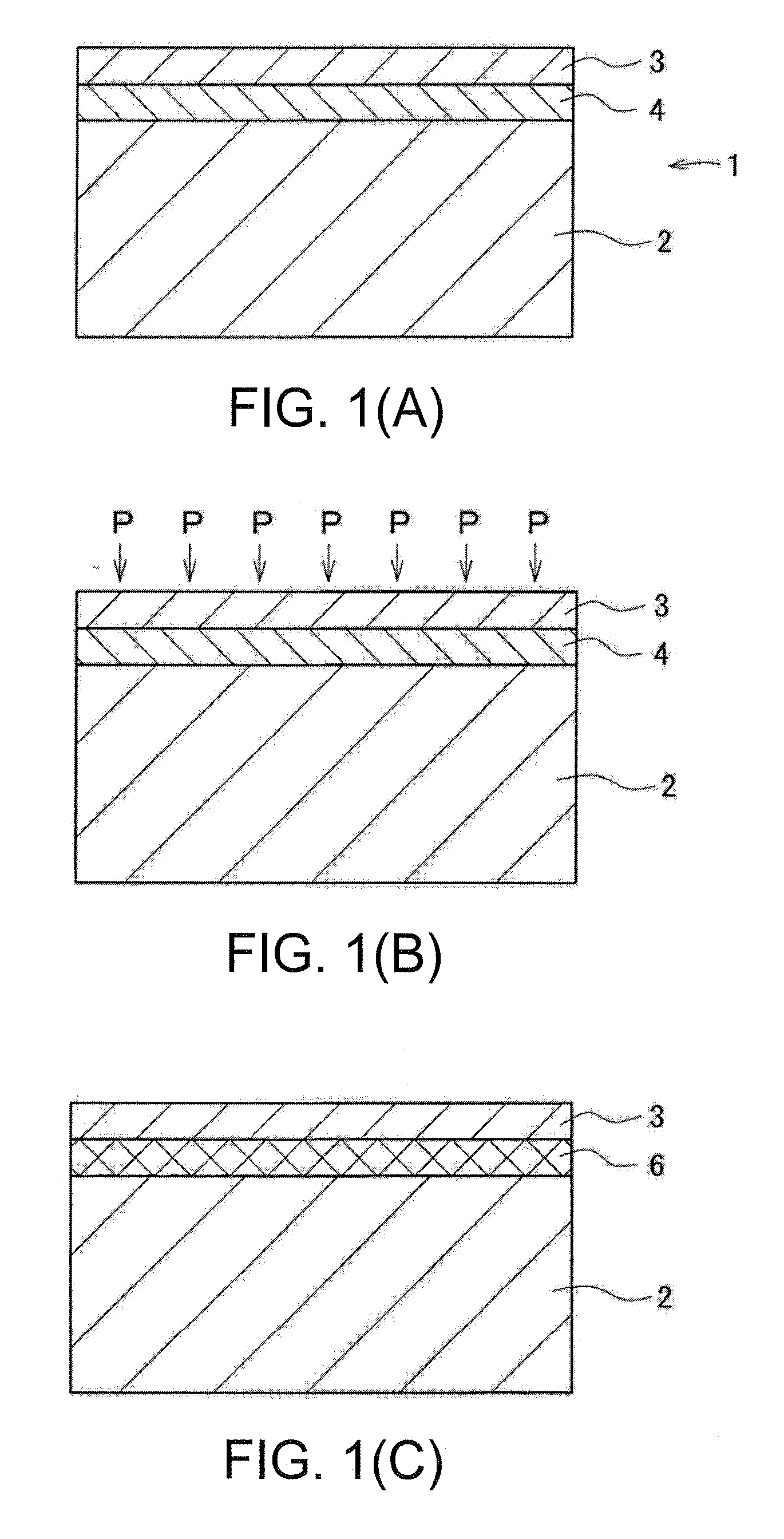
[0030]FIGS. 1(A) to 1(C) and FIGS. 2(D) to 2(F) are views showing a method for producing a single crystal SiC substrate according to a first embodiment of the invention.

[0031]The method for producing the single crystal SiC substrate performs Steps (1) and (2) below.

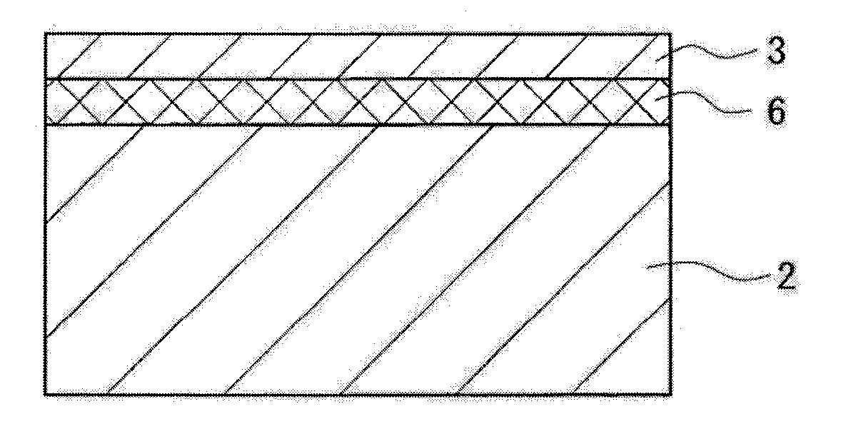
[0032](1) A P-type ion introduction step in which P-type ions are introduced from a side of a surface Si layer 3 to an SOI (Silicon On Insulator) substrate 1 in which a surface Si layer 3 and an embedded oxide layer 4 having a predetermined thickness are formed on an Si base material layer 2 to convert the embedded oxide layer 4 into a PSG layer 6 as an embedded glass layer and lower a softening point.

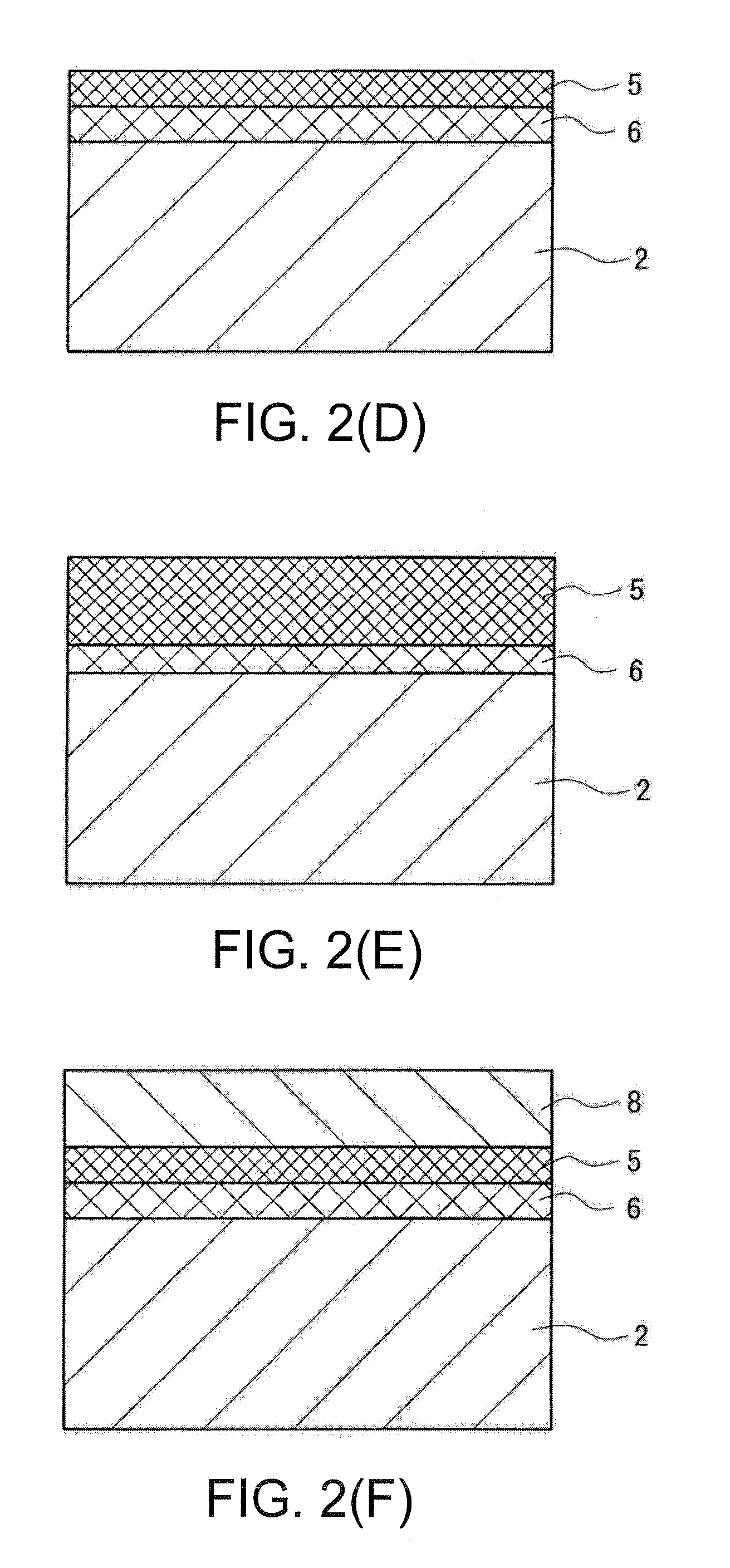
[0033](2) A SiC forming step in which the SOI substrate 1 having the PSG layer 6 as the above-mentioned embedded glass layer formed therein is heated in an atmosphere of hydrocarbon-based gas to convert the surface Si layer 3 into SiC, and thereafter, is cooled to form a single crystal SiC layer 5 on a surface thereof.

[0034]...

second embodiment

[0067]FIGS. 4(A) to 4(D) are diagrams showing a method for producing a single crystal SiC substrate according to a second embodiment of the invention.

[0068]The method for producing the single crystal SiC substrate performs Steps (1), (2) and (3) below.

[0069](1) A glass layer forming step of, before joining an Si base material and an Si thin plate constituting a surface Si layer, forming on a surface, to be a joint surface thereof, of at least one of the Si base material and the surface Si layer by a deposition method a glass layer having a softening point lower than at least the SiO2.

[0070](2) A joining step of joining the Si base material and the Si thin plate so as to sandwich the glass layer therebetween to form an embedded type substrate in which the Si base material layer, the surface Si layer and the embedded glass layer are laminated.

[0071](3) An SiC forming step of heating the embedded type substrate in an atmosphere of hydrocarbon-based gas to convert the surface Si layer i...


PUM

PropertyMeasurementUnit
temperatureaaaaaaaaaa
accelerating energyaaaaaaaaaa
thicknessaaaaaaaaaa

Abstract

A single crystal SiC substrate is produced with low cost in which a polycrystalline SiC substrate with relatively low cost is used as a base material substrate where the single crystal SiC substrate has less strain, good crystallinity and large size. The method including a P-type ion introduction step for implanting P-type ions from a side of a surface Si layer 3 into an SOI substrate 1 in which the surface Si layer 3 and an embedded oxide layer 4 having a predetermined thickness are foamed on an Si base material layer 2 to convert the embedded oxide layer 4 into a PSG layer 6 to lower a softening point, and an SiC forming step for heating the SOI substrate 1 having the PSG layer 6 formed therein in an atmosphere of hydrocarbon-based gas to convert the surface Si layer 3 into SiC, and thereafter, cooling the resulting substrate to foam a single crystal SiC layer 5 on a surface thereof.

Description

TECHNICAL FIELD[0001]The present invention relates to a method for producing a single crystal SiC substrate and the single crystal SiC substrate; specifically relates to a method for producing a single crystal SiC substrate in which a single crystal SiC substrate having a large size, good crystallinity and less strain can be produced, and the single crystal SiC substrate.RELATED ART[0002]Single crystal SiC (silicon carbide) is excellent in thermal and chemical stability, high in mechanical strength and resistant to irradiation, and due to these properties, has attracted an attention as a semiconductor device material for the next generation. Particularly, the single crystal SiC is considered to be promising in a technical field of substrate material such as a blue light emitting diode, an environmentally-resistant semiconductor device and the like. As a method for obtaining an SiC film used for such an application, there are generally used a liquid phase growth method at a temperatu...

Claims


Application Information

Patent Timeline
Patent Type & Authority Applications(United States)
IPC IPC(8): H01L29/24H01L21/22H01L21/04H01L33/32
CPCC30B1/10C30B29/36H01L21/02381H01L21/265H01L21/02529H01L21/02614H01L21/76251H01L21/02488
Inventor IZUMI, KATSUTOSHIYOKOYAMA, TAKASHI
Owner PUBLIC UNIVERSITY CORPORATION OSAKA CITY UNIVERSITY
Why Eureka
Try Eureka