


Quick Research
Generate reliable direction feasibility study reports for your R&D in just a few steps.

Technical Q&A
Discover and master advanced knowledge NOW. Basics, ideas, possibilities, all at once.

Find Solutions
As an expert in R&D theories, this can generate solutions to your technical problems instantly.

Evaluate Feasibility
Analyze your overall solution with one click, know your potential R&D risks in advance.

Monitor Landscape
Get weekly tech updates, stay abreast of the latest tech innovations and key insights.
Amplifying circuit and imaging device imaging device
- Summary
- Abstract
- Description
- Claims
- Application Information
AI Technical Summary
Benefits of technology
Problems solved by technology
Method used
Image

Examples
first embodiment
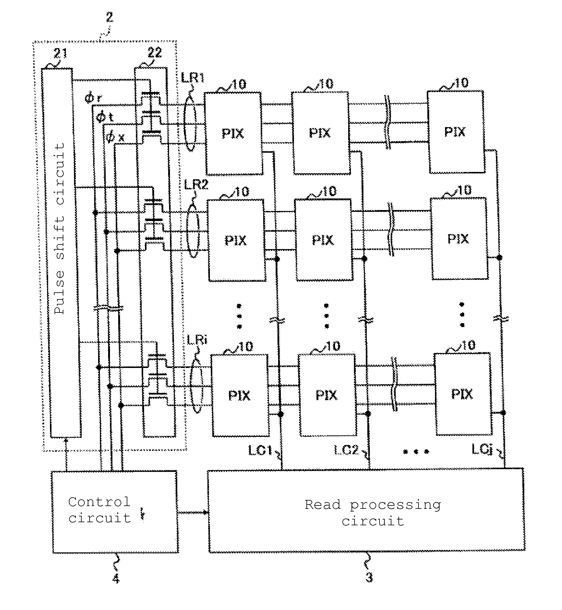
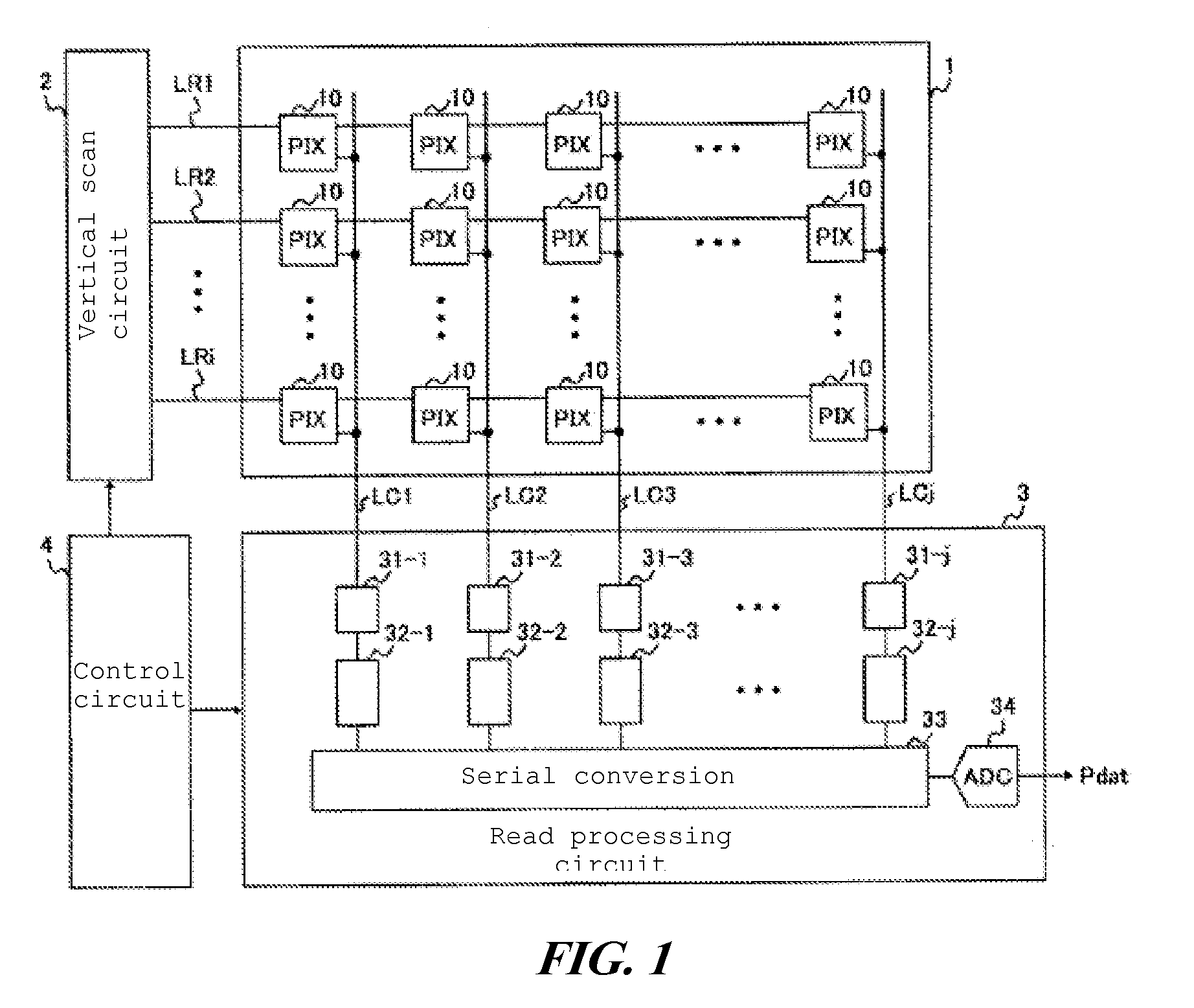
[0061]FIG. 1 shows an example of the configuration of an imaging device pertaining to the present invention. The imaging device pertaining to this embodiment has a pixel array 1, a vertical scan circuit 2, a read processing circuit 3, and a control circuit 4.
[0062]Pixel array 1 is an embodiment of the pixel array in the present invention.
[0063]Vertical scan circuit 2 is an embodiment of the pixel scan circuit in the present invention.
[0064]Pixel array 1 has multiple pixel circuits 10 that convert light from photographed subjects to electrical signals. Pixel circuits 10 are arranged in a matrix form, and are connected to common row signal lines LR1, LR2, . . . in each row, and are connected to common column signal lines LC1, LC2, . . . in each column.
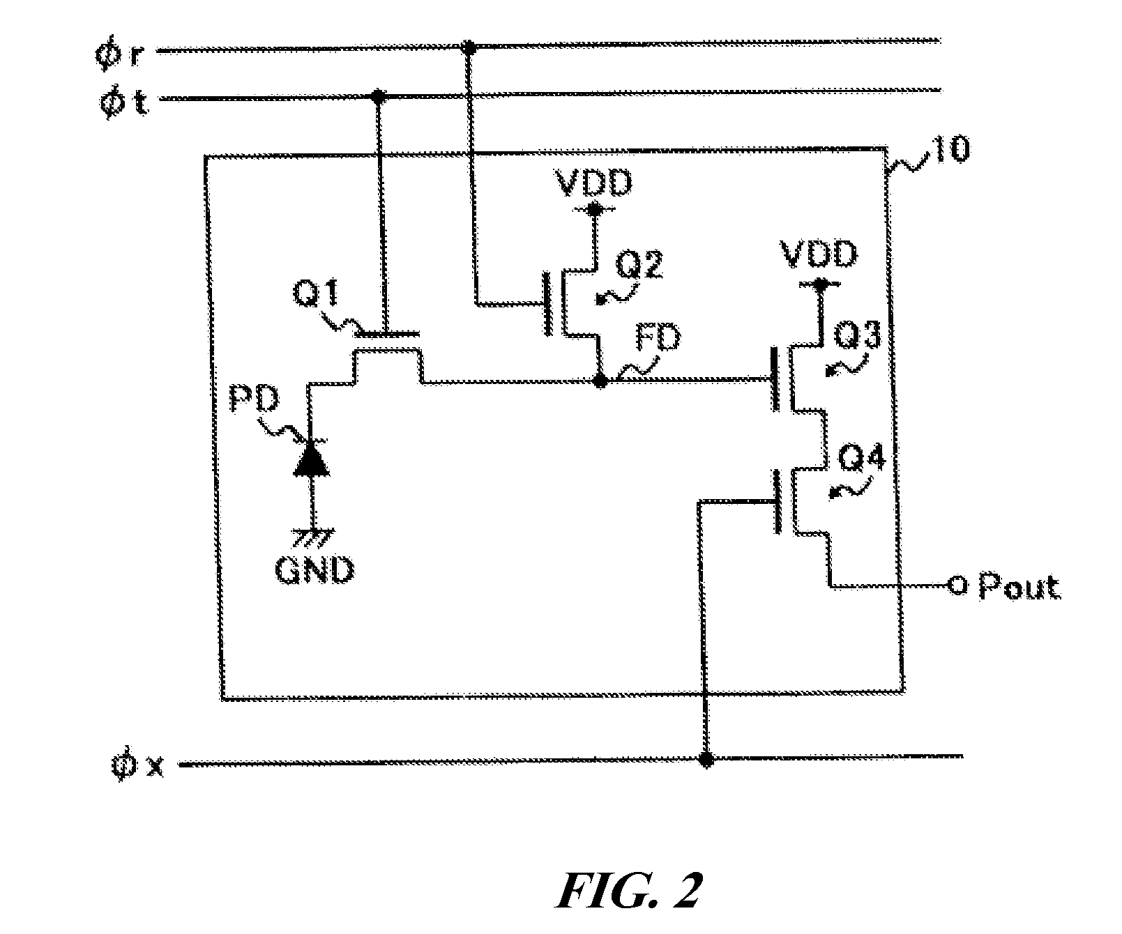
[0065]FIG. 2 shows an example of the configuration of pixel circuit 10. A pixel circuit 10 has a photodiode PD that receives light from a photographed subject to generate a light charge, and n-type MOS transistors Q1 to Q4.
[0066]The anod...
second embodiment
[0190]Next, the present invention will be explained.
[0191]With the imaging device pertaining to the second embodiment, read circuit 32 in the imaging device pertaining to the first embodiment (FIG. 5) is replaced with a read circuit 32A in which the capacitance of capacitor C1 is variable (FIG. 13).
[0192]With read circuit 32 shown in FIG. 5, gain is set according to the number of repetitions of the signal accumulation operations in the integration phase, but with read circuit 32A in this embodiment, gain can additionally be adjusted according to the capacitance ratio of capacitors C1 and C2.
[0193]FIG. 13 shows an example of the configuration of read circuit 32A.
[0194]Read circuit 32A shown in FIG. 13 has capacitor C1, which includes two unit capacitors connected in parallel between nodes N1 and N2, and switch circuits SW14 and SW15 provided in the conduction path between the unit capacitors and node N2. The other components in read circuit 32A are the same as read circuit 32 shown i...
third embodiment
[0200]Next, the present invention will be explained.
[0201]With the imaging device pertaining to the third embodiment, read circuit 32 in the imaging device pertaining to the first embodiment (FIG. 5) is replaced with read circuit 32B to which a dark level voltage VB can be input (FIG. 15).
[0202]With read circuit 32 shown in FIG. 5, the signal charge is integrated in the integration phase, but with read circuit 32B in this embodiment, a reference charge for setting the desired dark level is integrated, in addition to the signal charge.
[0203]FIG. 15 shows an example of read circuit 32B.
[0204]Read circuit 32B shown in FIG. 15 has a switch circuit SW13 to input dark level voltage VB to node N1. The other components of read circuit 32B are the same as read circuit 32 shown in FIG. 5.
[0205]With read circuit 32B shown in FIG. 15, in the integration phase, the signal charge is accumulated by repeating the first signal accumulation operation (FIG. 7, FIG. 9) and the second signal accumulatio...
PUM
 Abstract
Description
Claims
Application Information
 - R&D Engineer
- R&D Manager
- IP Professional
- Industry Leading Data Capabilities
- Powerful AI technology
- Patent DNA Extraction
Browse by: Latest US Patents, China's latest patents, Technical Efficacy Thesaurus, Application Domain, Technology Topic, Popular Technical Reports.
© 2024 PatSnap. All rights reserved.Legal|Privacy policy|Modern Slavery Act Transparency Statement|Sitemap|About US| Contact US: help@patsnap.com