Controller, data storage device and data storage system having the controller, and data processing method

a data storage device and controller technology, applied in computing, memory address/allocation/relocation, instruments, etc., can solve the problems of affecting the development and use affecting the speed of data processing, and affecting the development of a general hard disk file system. achieve the effect of improving the data processing speed

Active Publication Date: 2010-10-28
SAMSUNG ELECTRONICS CO LTD
View PDF12 Cites 100 Cited by
  • Summary
  • Abstract
  • Description
  • Claims
  • Application Information

AI Technical Summary

Benefits of technology

[0008]The present inventive concept provides a solid state drive (SSD) controller for improving a data processing speed by processing a plurality of instructions, such as a native command queue (NCQ), in parallel, a data storage device and a data storage system including the controller, and a data processing method.

Problems solved by technology

NOR flash memory is characterized by high speed access (reading) to stored data, but relatively slow writing speeds.
Unfortunately, the erase operation and the write operation are applied to different sized blocks of data (i.e., different unit operation sizes) within the flash memory.
This inherent unit operation size mismatch has traditionally impeded the use of flash memory in main memories, and has also hindered the development and use of a general hard disk file system when flash memory is used within an auxiliary storage device.
This conventional disability largely precludes the higher performance being demanded for contemporary semiconductor memory devices and related memory systems.
In other words, since conventional SSD controllers include only a single FTL to handle all of the data channels provided by a multi-channel parallel array structure, when a plurality of instructions are processed simultaneously in an NCQ environment, the instruction processing functionality of the FTL restricts overall performance of the constituent semiconductor memory devices, and limits the data access capabilities of the incorporating memory system.

Method used


Image

  • Controller, data storage device and data storage system having the controller, and data processing method
  • Controller, data storage device and data storage system having the controller, and data processing method
  • Controller, data storage device and data storage system having the controller, and data processing method

Examples


Embodiment Construction

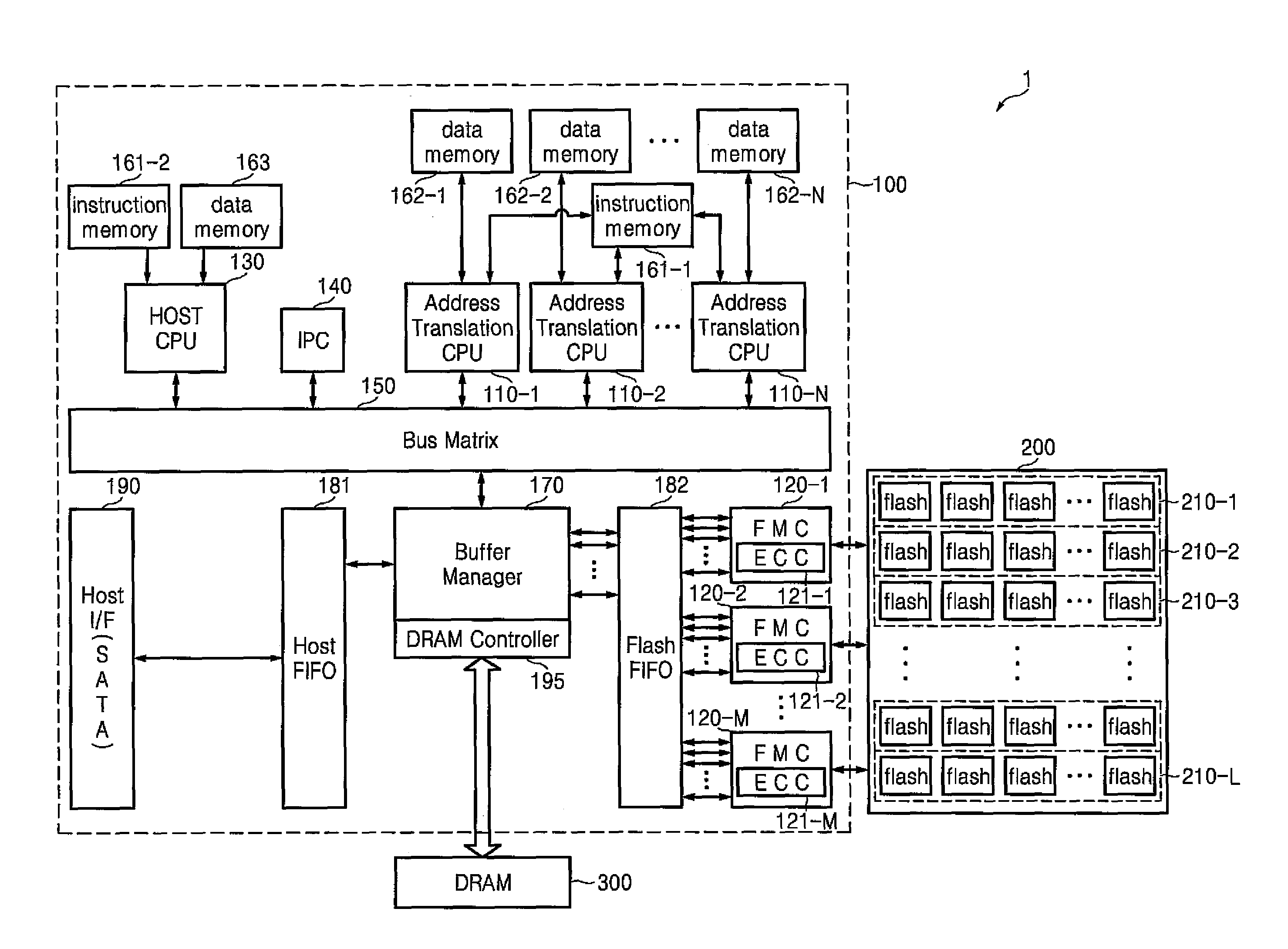
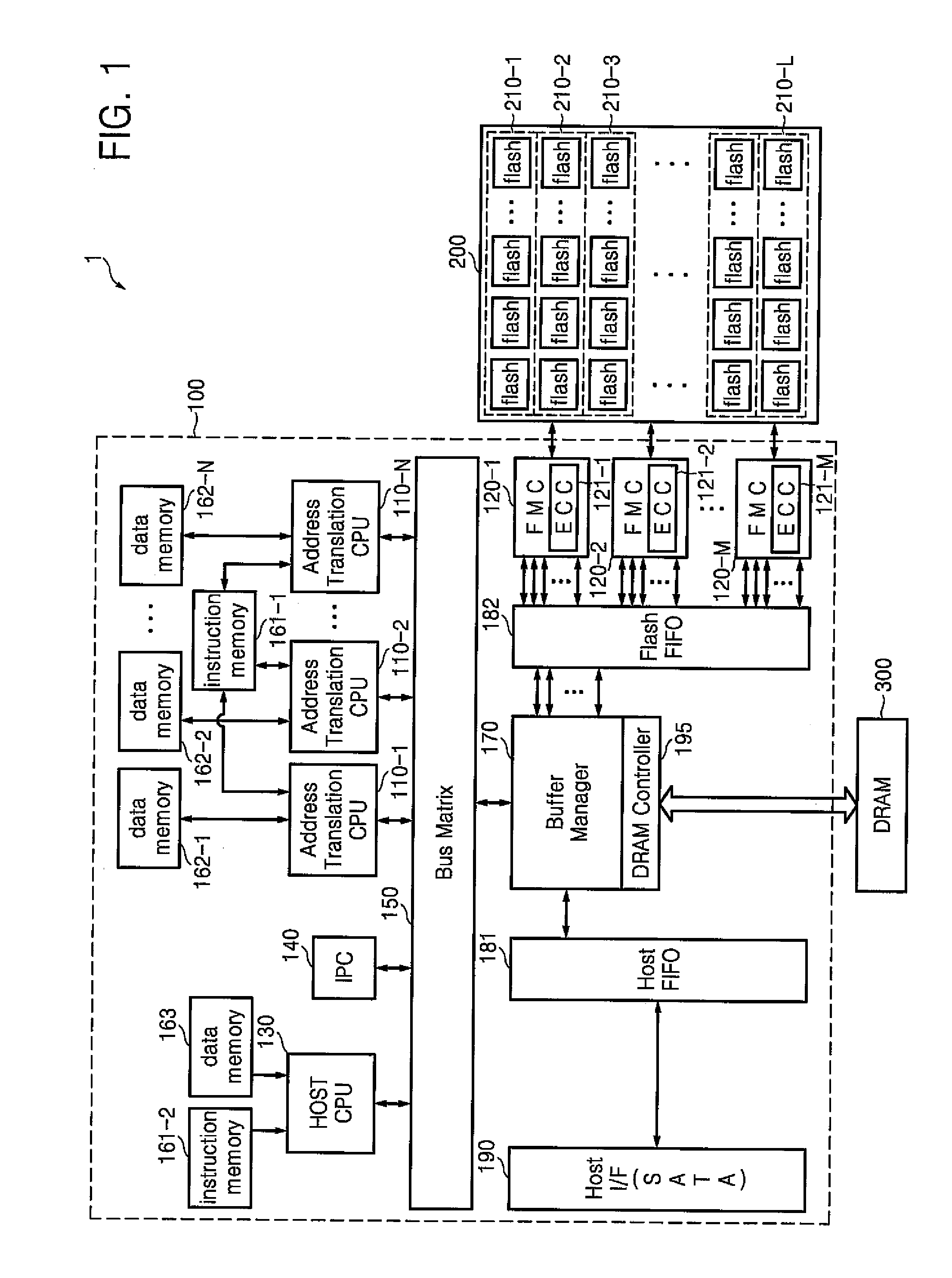
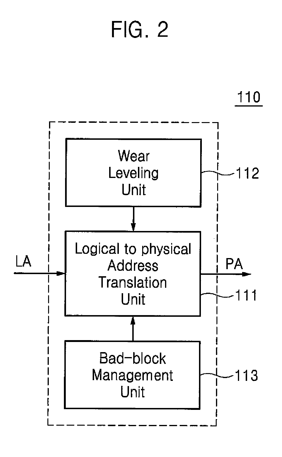
[0034]Figure (FIG. 1 is a schematic block diagram of a data storage system 1 according to an embodiment of the inventive concept. The data storage system 1 generally comprises a solid state disk (SSD) controller 100, a non-volatile memory device 200, and a random access memory 300. Although a SSD controller is used in the example of the data storage system of FIG. 1, the present inventive concept is not limited thereto.

[0035]The non-volatile memory device 200 comprises at least one non-volatile memory cell. The non-volatile memory cell may include EEPROM, flash memory, magnetic RAM (MRAM), spin-transfer torque MRAM, conductive bridging RAM (CBRAM), ferroelectric RAM (FeRAM), PRAM (phase change RAM), resistive RAM (RRAM or ReRAM), nanotube RRAM, polymer RAM (PoRAM), nano floating gate memory (NFGM), holographic memory, a molecular electronic memory device, or insulator resistance change memory. Each non-volatile memory cell may be configured to store a single bit of data or a plurali...


PUM


Abstract

A controller, a data storage device and a data storage system including the controller, and a data processing method are provided. The controller may process a plurality of instructions in parallel by including a plurality of address translation central processing units (CPUs) in a multi-channel parallel array structure, thereby improving the performance of a semiconductor memory system.

Description

CROSS-REFERENCE TO RELATED APPLICATIONS[0001]This application claims priority to Korean Patent Application No. 10-2009-0035077 filed on Apr. 22, 2009, the subject matter of which is hereby incorporated by reference.BACKGROUND[0002]The present inventive concept relates to storage devices, and more particularly to controllers improving the performance of semiconductor memory systems by processing a plurality of instructions in parallel by including a plurality of logical-to-physical address translation central processing units (CPUs) in a multi-channel parallel array structure. The inventive concept also relates to data storage devices and data storage systems including this type of controller, as well as associated data processing methods.[0003]Non-volatile memory is generally characterized by an ability to retain stored data in the absence of applied power. Flash memory is one type of non-volatile memory, and is widely used in computers, memory cards, and a variety of consumer elect...

Claims


Application Information

Patent Timeline
Patent Type & Authority Applications(United States)
IPC IPC(8): G06F12/00G06F12/02G06F12/10
CPCG06F12/0246G06F12/0292G06F12/02G06F13/10G06F13/16
Inventor LEE, TAE HACK
Owner SAMSUNG ELECTRONICS CO LTD
Why Eureka
Try Eureka