Laminated film and process for producing semiconductor device
a technology of laminate film and semiconductor device, which is applied in the direction of chemistry apparatus and processes, synthetic resin layered products, transportation and packaging, etc., can solve the problems of deteriorating peeling ability, complex product management, and difficulty in applying an appropriate amount of adhesive to the small wafer without damaging the wafer, etc., to achieve excellent storage stability, easy peeling of die-adhering layer, and effective fixation
- Summary
- Abstract
- Description
- Claims
- Application Information
AI Technical Summary
Benefits of technology
Problems solved by technology
Method used
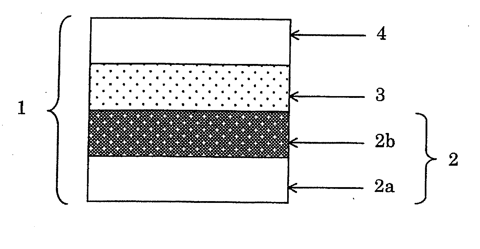
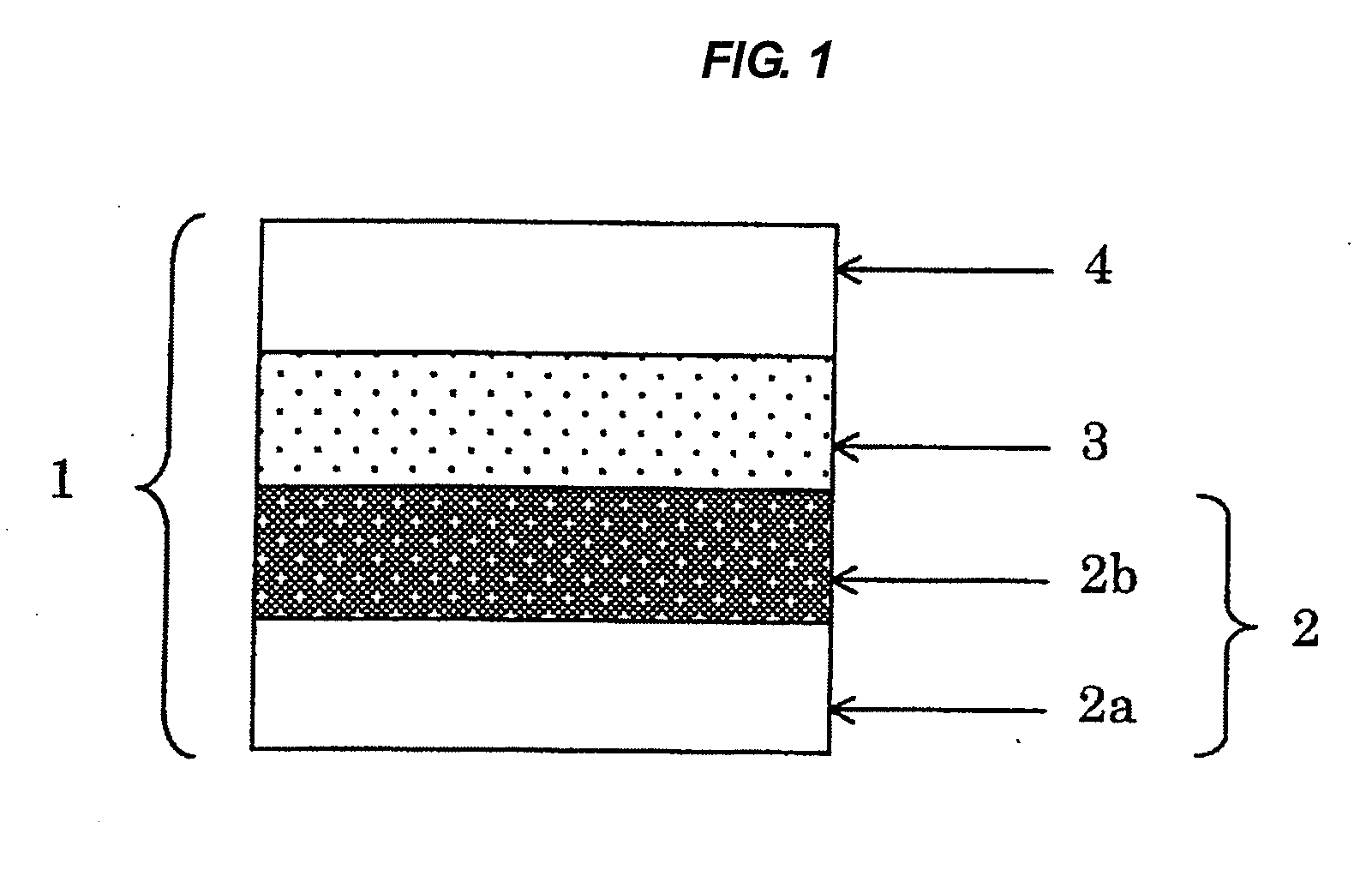
Image

Examples
example 1
(Manufacture of Pressure-Sensitive Adhesive Sheet)
[0129]An acrylic polymer was obtained by charging 96.8 parts by weight of 2-ethylhexyl acrylate (sometimes refers to as “2EHA”), 3.2 parts by weight of 2-hydroxyethyl acrylate (sometimes refers to as “HEA”), 0.2 part by weight of benzoyl peroxide, and 65 parts by weight of toluene into a reactor equipped with a condenser, a nitrogen-introducing pipe, a stirring apparatus, and a thermometer, and carrying out a polymerization reaction at 61° C. for 6 hours under a nitrogen atmosphere.
[0130]Next, a pressure-sensitive adhesive solution was prepared by adding 3.0 parts by weight of an isocyanate-based crosslinking agent (product name “COLONATE L” manufactured by Nippon Polyurethane Industry Co., Ltd.) and 4.0 parts by weight of a blocked isocyanate (product name “Takenate WB-700” manufactured by Mitsui Chemical Polyurethane Industries, Ltd.; blocking agent dissociation temperature: 120° C.) to 100 parts by weight of the acrylic polymer.
[0...
examples 2 to 5
[0134]Pressure-sensitive adhesive sheets fitted with a die-adhering layer (laminated films) were manufactured in the same manner as in Example 1 except that the composition of the pressure-sensitive adhesive composition was changed to the composition (kind and content of monomer components) shown in Table 1.
PUM
 Abstract
Description
Claims
Application Information
 - R&D Engineer
- R&D Manager
- IP Professional
- Industry Leading Data Capabilities
- Powerful AI technology
- Patent DNA Extraction
Browse by: Latest US Patents, China's latest patents, Technical Efficacy Thesaurus, Application Domain, Technology Topic.
© 2024 PatSnap. All rights reserved.Legal|Privacy policy|Modern Slavery Act Transparency Statement|Sitemap