Solar cell and method of manufacturing the same

a solar cell and photoelectric technology, applied in the field of solar cells, can solve the problems of increasing social costs, air pollution and environmental damage, and the shortage of fossil fuel supply, and achieve the effect of enhancing the photoelectric performance of solar cells

Inactive Publication Date: 2010-11-11
IND TECH RES INST
View PDF7 Cites 18 Cited by
  • Summary
  • Abstract
  • Description
  • Claims
  • Application Information

AI Technical Summary

Benefits of technology

[0010]The present invention provides a solar cell with photonic crystals so as to enhance the photoelectric performance of the solar cell.

Problems solved by technology

The supply of fossil fuels faces the shortage problem, and the combustion of fossil fuels leads to the air pollution and environmental damage.
Nuclear energy can provide high electricity density, but it has the safety concern about the radiation and the storage of nuclear waste.
Both of the above-mentioned energy increases the social cost.
Solar energy is clean and inexhaustible with few limitations.
However, the foregoing system may undergo cost issue and have system dimension problem which will limit the development of the system.
In GaN-based system, most of the devices are fabrication in lateral structure due to the sapphire substrate, which has low conductivity, low thermal resistance and large lattice mismatch with epi-layer.
However, the increase of the absorption thickness means higher cost and heavy device.
Thus, the opto-electric conversion efficiency is also reduced.

Method used


Image

  • Solar cell and method of manufacturing the same
  • Solar cell and method of manufacturing the same
  • Solar cell and method of manufacturing the same

Examples


first embodiment

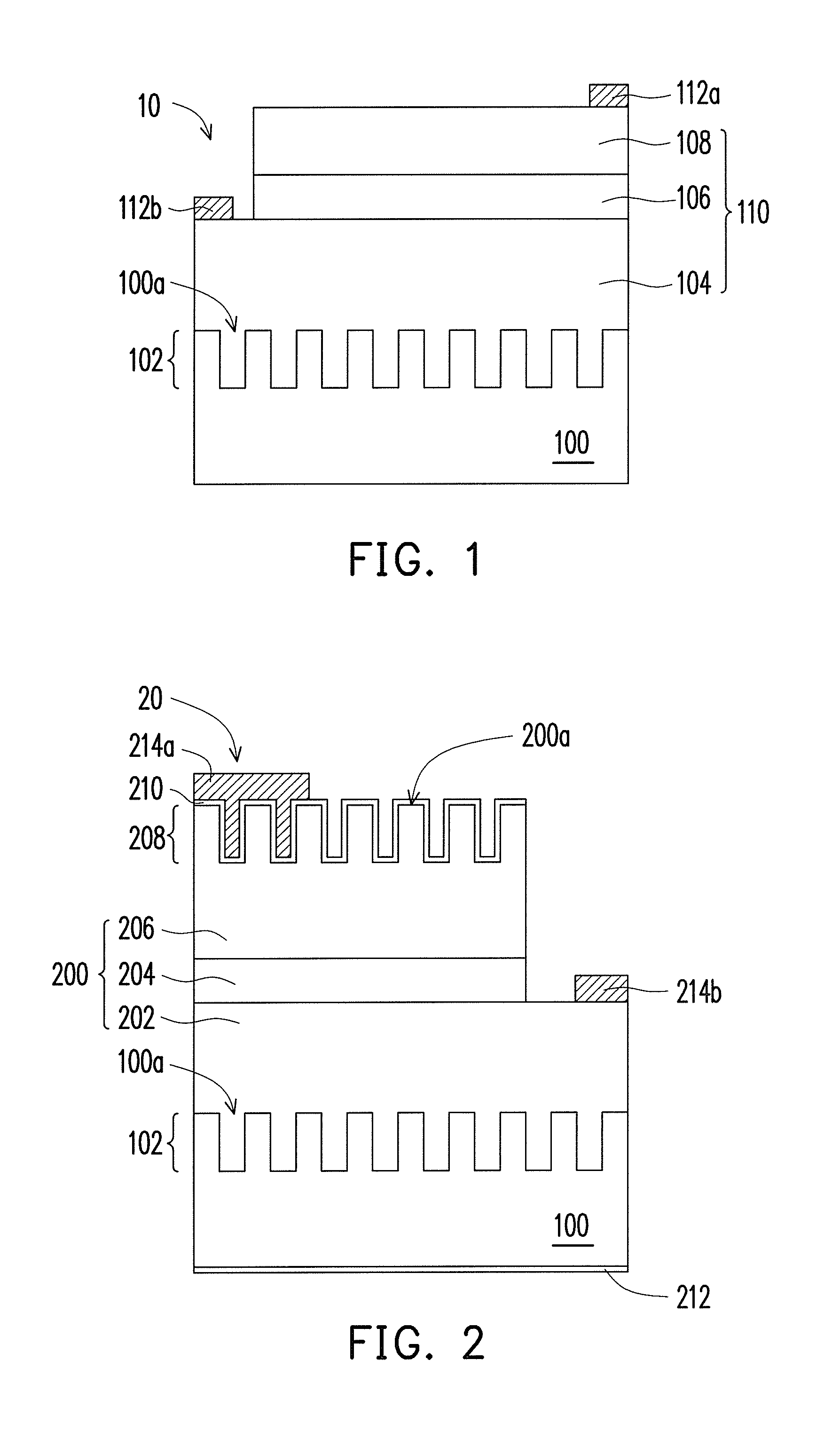
[0031]A schematic diagram of a solar cell of the present invention is shown in FIG. 1. The solar cell is group III-V compound solar cell, for example. FIG. 1 shows a lateral view of the solar cell 10, which includes a substrate 100 having a surface 100a with photonic crystals 102, a multilayer semiconductor layer 110, a first electrode 112a and a second electrode 112b. The substrate 100 includes sapphire, GaAs, Ge, Si, SiGe or the other materials, for example. The multilayer semiconductor layer 110 is disposed on the surface 100a of the substrate 100, and the first electrode 112a and the second electrode 112b are respectively disposed on different conduction-type portions of the multilayer semiconductor layer 110. For example, an arrangement of the photonic crystals 102 includes periodic, quasi-periodic or non-periodic arrangement, in which the periodic arrangement may include four-fold rotational symmetry or six-fold rotational symmetry. Moreover, the photonic crystals 102 may be p...

second embodiment

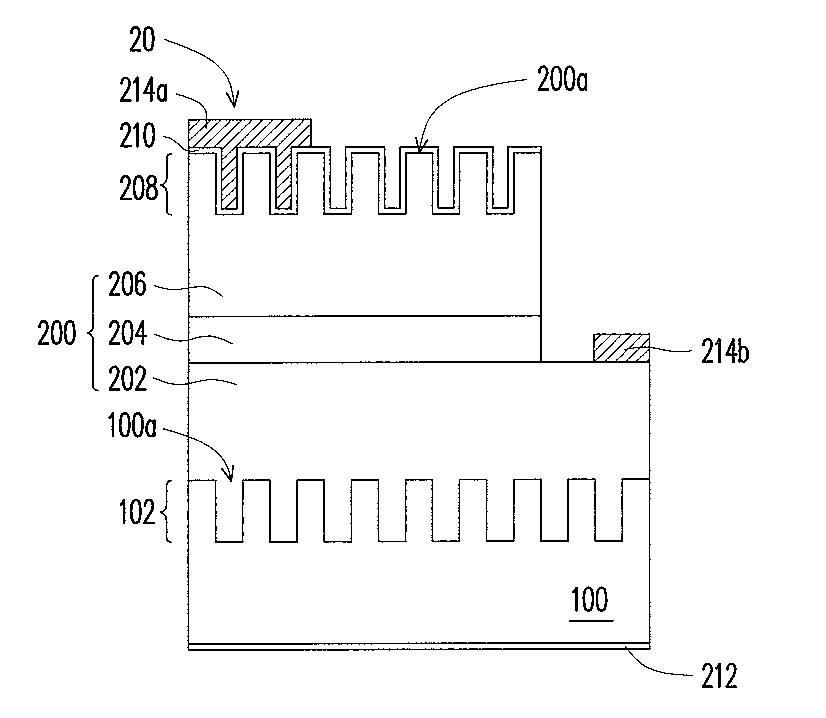
[0033]For further explanation, a schematic diagram of a solar cell of the present invention is shown in FIG. 2. FIG. 2 shows a solar cell 20 similar to that in FIG. 1, and the same numbers represent the same elements in FIGS. 1 and 2. The solar cell 20 includes a substrate 100 having a surface 100a with photonic crystals 102 and a multilayer semiconductor layer 200, wherein the multilayer semiconductor layer 200 has a top surface 200a with other photonic crystals 208. In addition, an arrangement of the photonic crystals 208 includes periodic, quasi-periodic or non-periodic arrangement, in which the periodic arrangement may include four-fold rotational symmetry or six-fold rotational symmetry. Moreover, the photonic crystals 208 may be produced by Laser interferometric lithography, electron beam lithography or Nanoimprint. When a light is incident to the solar cell 20 from the top surface 200a with first kind photonic crystal 102 functioned as surface texture surface, the light may e...

third embodiment

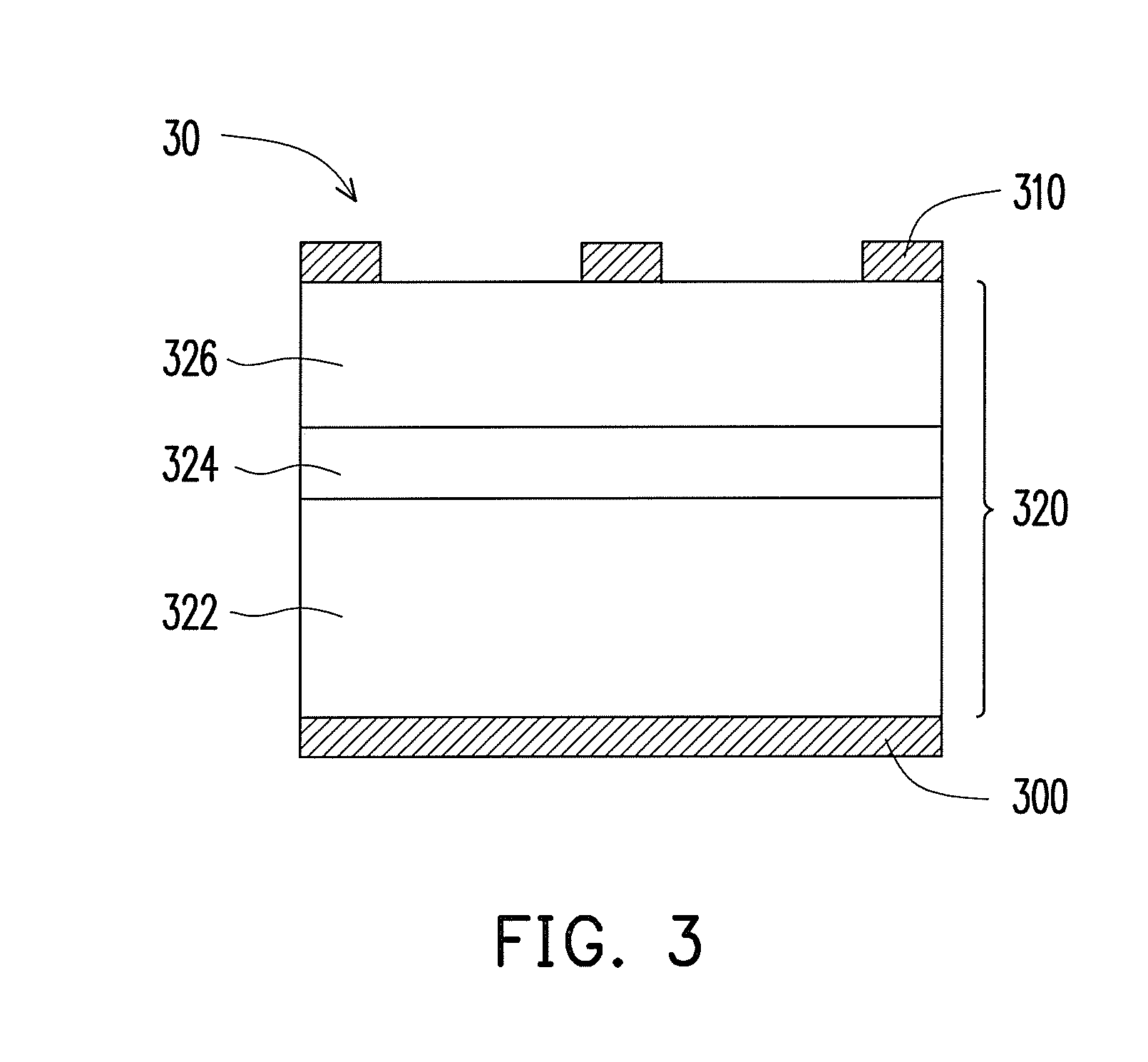
[0035]A schematic diagram of a GaN-based solar cell of the present invention is shown in FIG. 3. FIG. 3 shows a GaN-based solar cell 30 that includes a first electrode 300, a second electrode 310, and a multilayer semiconductor layer 320 having at least one active layer 324, wherein a material of the multilayer semiconductor layer 320 is a GaN-based semiconductor or alloy thereof, such as GaN, InN, AlN, InGaN, AlGaN, AlInGaN and so on. In FIG. 3, the multilayer semiconductor layer 320 includes a first conductive type semiconductor 322, the active layer 324, and a second conductive type semiconductor 326, for example. The first electrode 300 is disposed on a surface of the first conductive type semiconductor 322, and the second electrode 310 is disposed on a surface of the second conductive type semiconductor 326 opposite to the first electrode 300. Furthermore, the multilayer semiconductor layer 320 includes a p-n or a p-i-n structure. A type of the first electrode 300 and the secon...


PUM


Abstract

A bi-functional photovoltaic device is provided. The bi-functional photovoltaic device includes at least one solar cell and a control device. Each of the solar cell includes a multilayer semiconductor layer of group III-V compound semiconductor, a first electrode disposed on the back of the multilayer semiconductor layer, and a second electrode disposed on the front of the multilayer semiconductor layer. The control device connects with the at least one solar cell in order to control them functioning as solar cell or light emitting diode.

Description

BACKGROUND OF THE INVENTION[0001]1. Field of Invention[0002]The present invention relates to a solar cell for improving properties thereof.[0003]2. Description of Related Art[0004]The supply of fossil fuels faces the shortage problem, and the combustion of fossil fuels leads to the air pollution and environmental damage. Nuclear energy can provide high electricity density, but it has the safety concern about the radiation and the storage of nuclear waste. Both of the above-mentioned energy increases the social cost. Therefore, renewable energy becomes the focus in terms of energy saving and pollution reducing. Many nations have started to develop and invest in the renewable energy and the feasibility as alternative energy.[0005]Photovoltaic (PV) modules of photoelectric conversion devices become the mainstream of alternative energy. Solar cells (or photovoltaic cells) which can convert solar energy directly into electricity are under intensive study. Solar energy is clean and inexha...

Claims


Application Information

Patent Timeline
Patent Type & Authority Applications(United States)
IPC IPC(8): H01L31/0256H01L31/00H01L31/02H01L31/18
CPCH01L25/167H01L31/056H01L31/0203H01L31/0232H01L31/0236H01L31/0304H01L31/03046H01L31/0693H01L31/075H01L31/184H01L31/1844H01L31/1852H01L33/20H01L33/32H01L33/382Y02E10/544Y02E10/548Y02E10/52H01L2924/0002H01L31/02021H01L2924/00H01L31/03044H01L31/03048H01L31/077H01L31/1892H01L31/054Y02E10/547Y02P70/50
Inventor WU, MING-HSIENYEH, WEN-YUNGXUAN, RONGLIAO, WEN-YIHHSU, JUNG-TSUNGCHU, MU-TAO
Owner IND TECH RES INST
Why Eureka
Try Eureka