Epitaxial substrate for semiconductor device, semiconductor device, and method of manufacturing epitaxial substrate for semiconductor device

Active Publication Date: 2010-11-18
NGK INSULATORS LTD
View PDF28 Cites 6 Cited by
  • Summary
  • Abstract
  • Description
  • Claims
  • Application Information

AI Technical Summary

Benefits of technology

[0017]Thereby, the temperature is lowered to the formation temperature of the barrier layer after forming the spacer layer, preventing deteriorati

Problems solved by technology

This deteriorates the quality of film and aggravates the surface morphology (e.g. increase of distortion, generation of cracks, and the like).
As a result, various problems have been caused, such that high concentration of two dimensional electron gas is not obtained as expected, various contact characteristics such as ohmic characteristic, Schottky characteristic and the like is deteriorated and unnecessary surface l

Method used


Image

  • Epitaxial substrate for semiconductor device, semiconductor device, and method of manufacturing epitaxial substrate for semiconductor device
  • Epitaxial substrate for semiconductor device, semiconductor device, and method of manufacturing epitaxial substrate for semiconductor device
  • Epitaxial substrate for semiconductor device, semiconductor device, and method of manufacturing epitaxial substrate for semiconductor device

Examples


##ventive example 1

Inventive Example 1

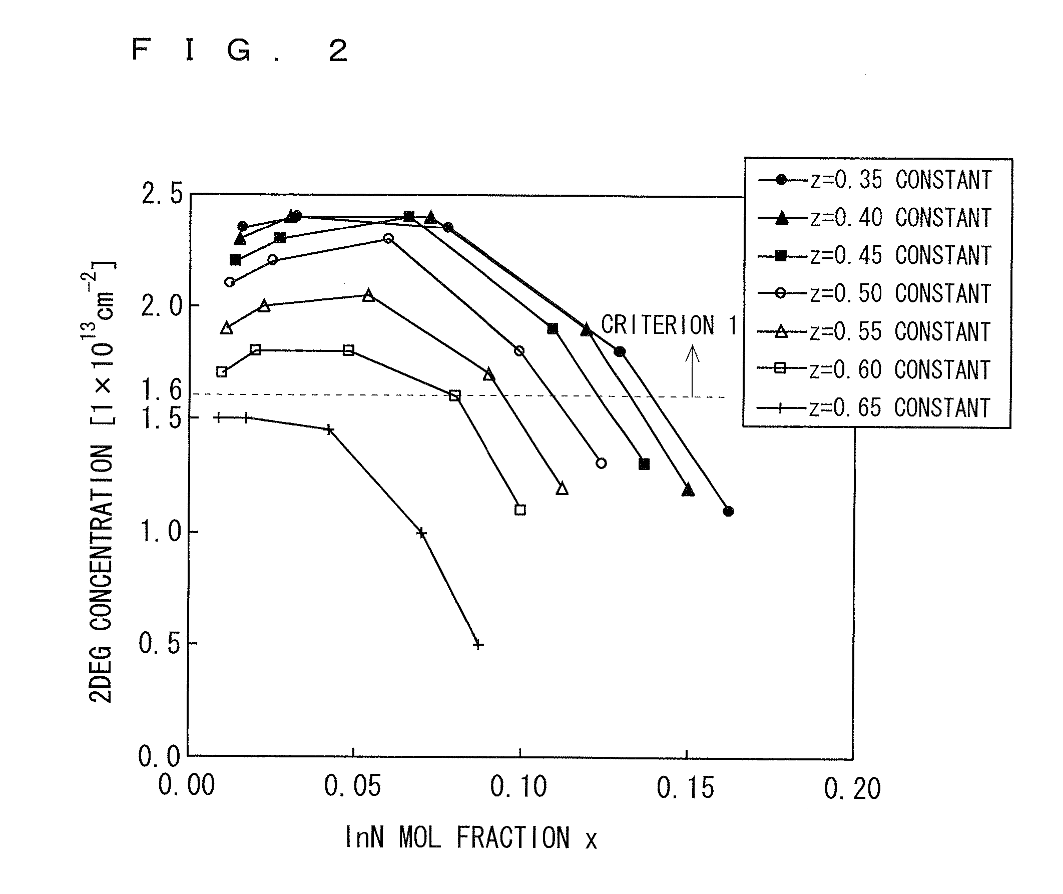
[0073]In the present inventive example, the HEMT device 10 according to the above preferred embodiment was manufactured. FIG. 7 is a view showing a list of the combinations of the composition of the barrier layer 5 in manufacturing the HEMT device 10 and the results of measuring the two dimensional electron gas concentration (2DEG concentration), the two dimensional electron gas mobility (2DEG mobility), the contact resistance, and the gate leakage current with respect to the resultant HEMT devices 10. In the present inventive example, 35 different types of the HEMT devices 10 were manufactured.

[0074]First, a (0001) plane sapphire substrate with 2 inch diameter was prepared as the substrate 1 to start manufacturing the epitaxial substrate 10A used for each of the HEMT devices 10. The substrate 1 was placed in the reactor of the MOCVD furnace and the atmosphere in the reactor was vacuumed. Thereafter, the pressure in the reactor was set to be 30 kPa and the atmosph...

##ventive example 2

Inventive Example 2

[0090]In the present inventive example, four types of the HEMT devices were manufactured by the same procedure as the inventive example 1 other than intentionally mixing hydrogen into the atmosphere gas in manufacturing the barrier layer 5, and the two dimensional electron gas concentration was measured. The target composition of the barrier layer 5 was In0.06Al0.44Ga0.5N. FIG. 8 is a view showing a list of measurement results of the two dimensional electron gas concentration of each HEMT device and ways of mixing hydrogen in the process of forming the barrier layer 5, the methods being employed in manufacturing the HEMT device according to the present inventive example. FIG. 8 also shows the measurement results of the two dimensional electron gas concentration of the HEMT devices in the inventive example 1 with the barrier layer 5 having the same composition as the present inventive example.

[0091]As shown in FIG. 8, the two dimensional electron gas concentration ...

##ventive example 3

Inventive Example 3

[0092]In the present inventive example, nine types of HEMT devices were manufactured by the same procedure as the inventive example 1 other than differentiating the formation temperatures of the channel layer 3, the spacer layer 4, and the barrier layer 5. The target composition of the barrier layer 5 was In0.06Al0.04Ga0.5N. The two dimensional electron gas concentration and mobility, the contact resistance, and the gate leakage current of the resultant HEMT device were measured. FIG. 9 is a view showing a list of the measurement results of the above each measurement and the formation temperature of each layer employed in manufacturing the HEMT devices according to the present inventive example. FIG. 9 also shows the measurement results of the HEMT device according to the inventive example 1 with the barrier layer 5 having the same composition as the present inventive example. In FIG. 9, the crosses are put to the measurement results not satisfying the device char...


PUM


Abstract

An epitaxial substrate having preferable two dimensional electron gas characteristic and contact characteristic is provided in the present invention. A channel layer is formed on a base substrate with GaN. A spacer layer is formed on the channel layer with AlN. A barrier layer is formed on the spacer layer with group III nitride having a composition of InXAlyGazN (wherein x+y+z=1) and at least including In, Al, and Ga such that the composition of the barrier layer is within the range surrounded with four lines defined in accordance with the composition on a ternary phase diagram with InN, AlN, and GaN as vertexes.

Description

BACKGROUND OF THE INVENTION[0001]1. Field of the Invention[0002]The present invention relates to an epitaxial substrate having a multi-layered structure and composed of a group III nitride semiconductor device, and particularly relates to an epitaxial substrate having a multi-layered structure for electronic devices and a method of manufacturing the same.[0003]2. Description of the Background Art[0004]Nitride semiconductors having higher breakdown electric field and higher electron saturation velocities have been drawing attention as the next generation semiconductor materials for high-frequency and high-power devices. Particularly, because a multi-layered structure formed by laminating layers composed of AlGaN and GaN is characterized in generating a two dimensional electron gas (2DEG) having high concentration in a lamination interface (heterointerface) by large polarization effect (spontaneous polarization effect and piezo polarization effect) specific to nitride material, the de...

Claims


Application Information

Patent Timeline
IPC IPC(8): H01L29/20H01L21/784H01L27/12
CPCC30B19/00C30B23/02C30B25/02C30B29/403C30B29/406H01L29/7786H01L21/0242H01L21/02458H01L21/0254H01L21/0262H01L29/2003H01L21/0237
Inventor ICHIMURA, MIKIYAMIYOSHI, MAKOTOTANAKA, MITSUHIRO
Owner NGK INSULATORS LTD
Why Eureka
Try Eureka