

Electron emitting element, electron emitting device, light emitting device, image display device, air blowing device, cooling device, charging device, image forming apparatus, electron-beam curing device, and method for producing electron emitting element
- Summary
- Abstract
- Description
- Claims
- Application Information
AI Technical Summary
Benefits of technology
Problems solved by technology
Method used
Image

Examples
embodiment 1
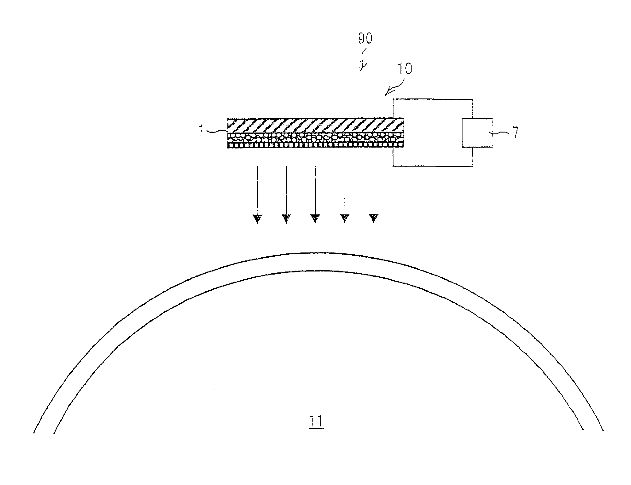
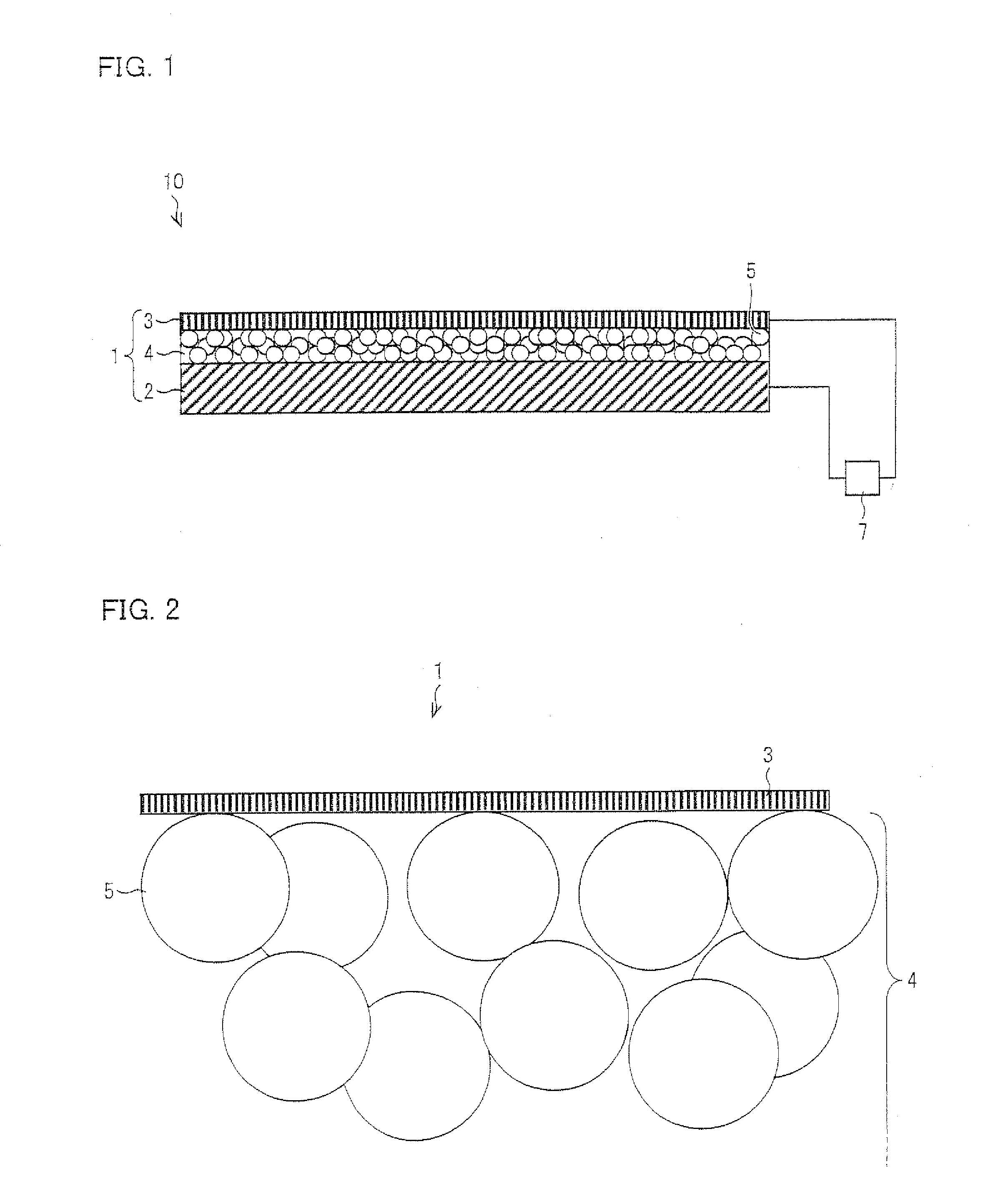
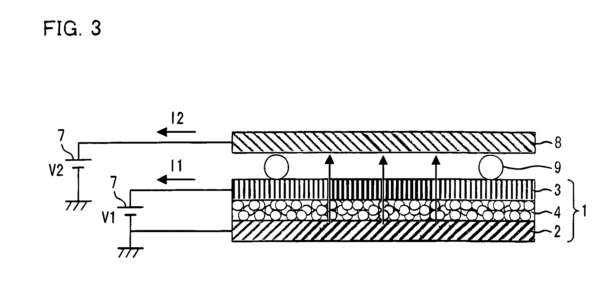
[0034]FIG. 1 is a schematic view illustrating an embodiment of an electron emitting device including an electron emitting element of the present invention. As illustrated in FIG. 1, an electron emitting element 1 of the present embodiment includes an electrode substrate 2 serving as a lower electrode, a thin-film electrode 3 serving as an upper electrode, and an electron acceleration layer 4 sandwiched between the electrode substrate 2 and the thin-film electrode 3. Further, the electrode substrate 2 and the thin-film electrode 3 are connected to a power supply 7, so that a voltage can be applied between the electrode substrate 2 and the thin-film electrode 3 which are provided so as to face each other. The electron emitting element 1 applies a voltage between the electrode substrate 2 and the thin-film electrode 3 so that current flows between the electrode substrate 2 and the thin-film electrode 3, that is, in the electron acceleration layer 4. A part of electrons in the current a...
example 1
[0075]First, four reagent bottles in which 3 mL of ethanol was supplied as a solvent were prepared. Then, 0.15 g, 0.25 g, 0.35 g, 0.50 g of silica particles (average particle diameter: 110 nm, specific surface area: 30 m2 / g) which were surface-treated with hexamethyldisilazane (HMDS) were added as the insulating fine particles 5 to the four reagent bottles, respectively. Subsequently, each of the reagent bottle was set in an ultrasonic dispersion device so that silica particle dispersion solutions A, B, C, and D each having a different concentration were produced.
[0076]Next, four 25-mm square SUS substrates were prepared as the electrode substrates 2. On the respective SUS substrates, the silica particle dispersion solutions A, B, C, and D were dropped and respective electron acceleration layers A, B, C, and D were formed by the spin coating method. A condition of the film formation by the spin coating method was such that (i) first the silica particle dispersion solutions A, B, C, ...
example 2
[0084]First, four reagent bottles were prepared. Into the four reagent bottles, respectively supplied were (i) 0.15 g of silica particles having a particle diameter of 12 nm (specific surface area: 200 m2 / g), (ii) 0.15 g of DDS-treated particles obtained by treating, with dimethyldichlorosilane (DDS), surfaces of the silica particles having an average particle diameter of 12 nm, (iii) 0.15 g of HMDS-treated particles obtained by treating, with hexamethyldisilazane (HMDS), the surfaces of the silica particles having an average particle diameter of 12 nm, and (iv) 0.15 g of silicone-oil-treated particles obtained by treating, with silicone oil, the surfaces of the silica particles having an average particle diameter of 12 nm. Then, 0.6 mL of ethanol as a solvent was added to each of the reagent bottles. Subsequently, each of the reagent bottles was set in an ultrasonic dispersion device so that silica particle dispersion solutions E, F, G, and H were produced.
[0085]By using the silica...
PUM
 Abstract
Description
Claims
Application Information