Electronic device, conductive composition, metal filling apparatus, and electronic device manufacturing method

US20100301485A1Active Publication Date: 2010-12-02NAPRA

Image

  • Electronic device, conductive composition, metal filling apparatus, and electronic device manufacturing method
  • Electronic device, conductive composition, metal filling apparatus, and electronic device manufacturing method
  • Electronic device, conductive composition, metal filling apparatus, and electronic device manufacturing method

Examples


first embodiment

(1) First Embodiment

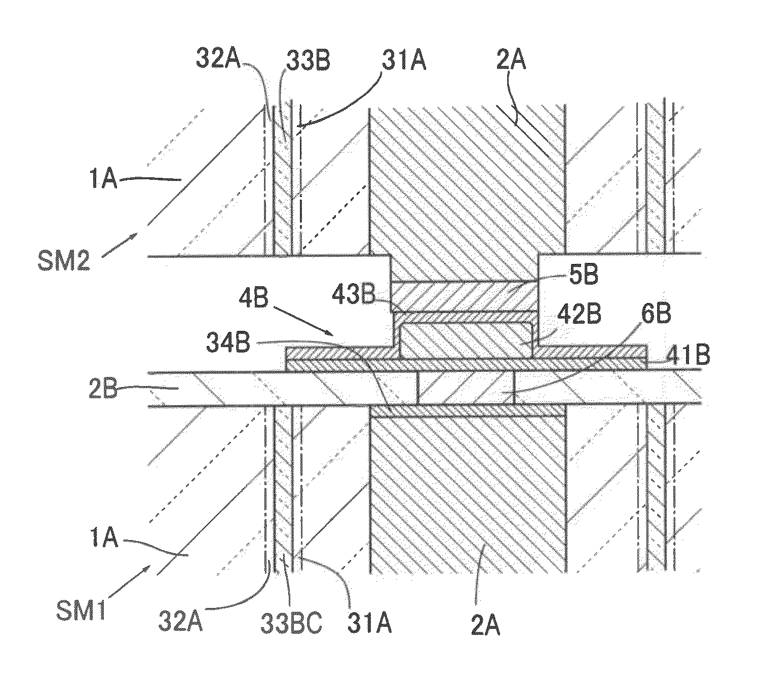
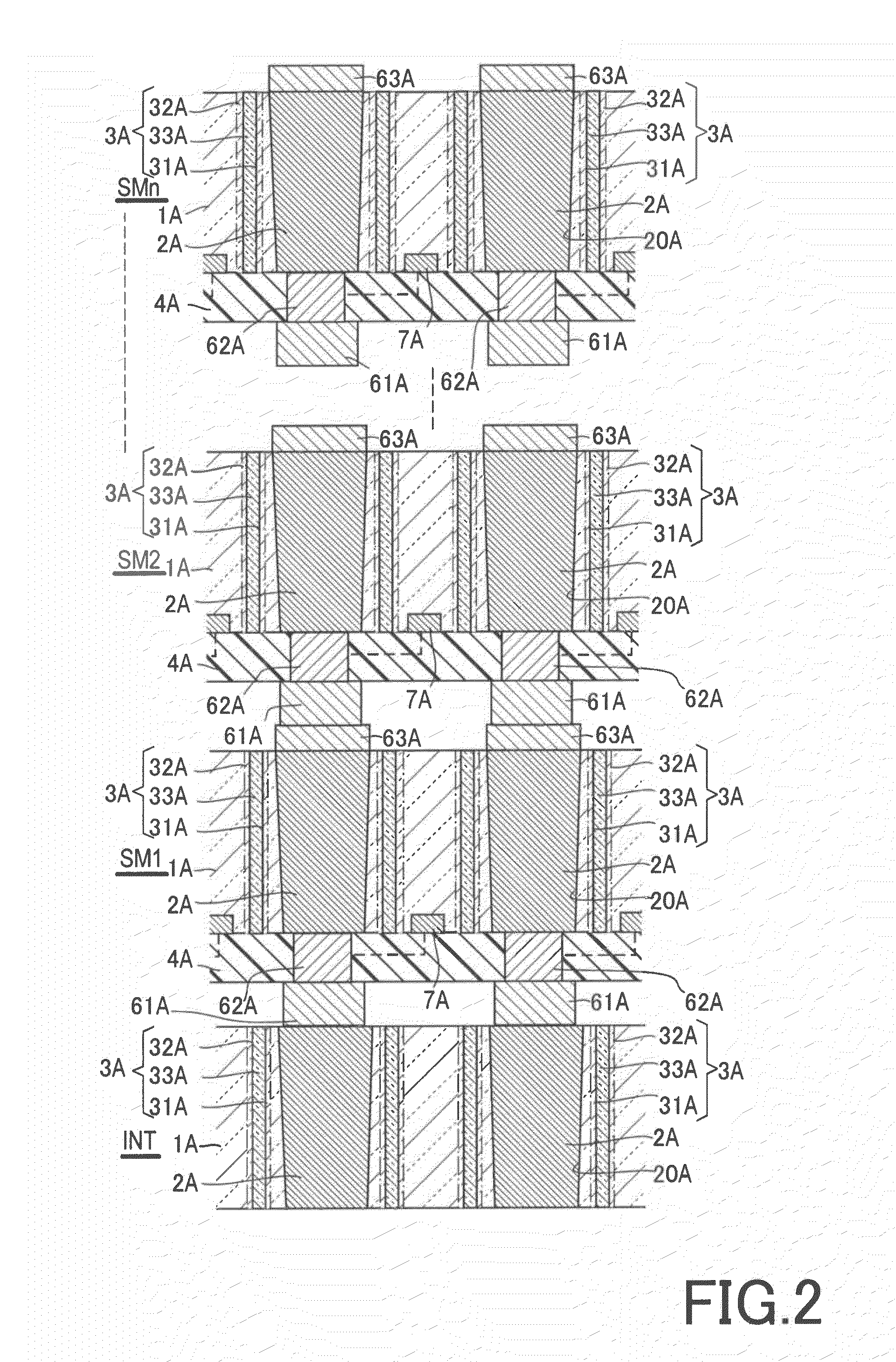
[0217]Referring to FIG. 17, a columnar conductor 3 fills a minute space 30 extending along the thickness direction from one surface of a substrate 1. At the bottom of the minute space 30, one end of the columnar conductor 3 is opposed to a film surface of a first conductor 2 across a junction film 4.

[0218]Although FIG. 17 illustrates the case where a single columnar conductor 3 is provided for a single first conductor 2, it should not be construed as limited thereto. It is also possible to provide a plurality of columnar conductors 3 for a single first conductor 2.

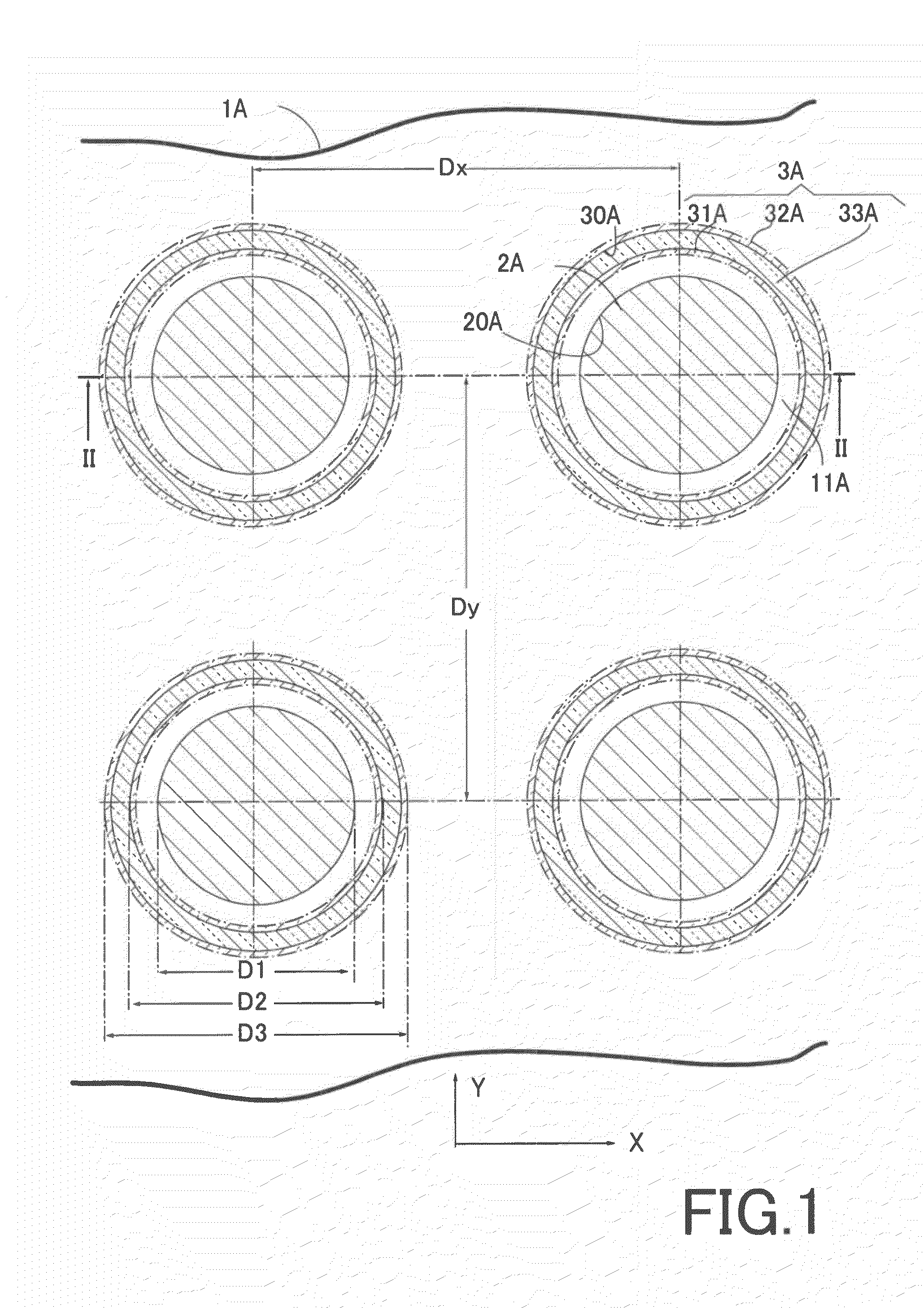
[0219]The minute space 30 filled with the columnar conductor 3 is a through-hole, a non-through-hole (blind hole), or a via hole. While the minute space 30 has a hole diameter of, for example, 60 μm or less, the thickness of the wafer itself is typically tens of μm. Accordingly, the minute space 30 has a considerably high aspect ratio.

[0220]Referring to FIG. 17, the first conductor 2 is formed flat on t...

second embodiment

(2) Second Embodiment

[0234]FIG. 25 is a view showing another embodiment of a substrate to be used for an electronic device according to the present invention. The present embodiment is characterized in that the junction film 4 is joined to almost the entire peripheral surface of the columnar conductor 3 within the minute space 30. The junction film 4 may be formed by a thin-film formation technology such as sputtering.

[0235]In the embodiment shown in FIG. 25, since the metal element contained in the junction film 4 is diffused into the columnar conductor 3 to create the alloy area AL over the entire peripheral surface of the columnar conductor3, mutual junction strengths between the first conductor 2, the columnar conductor 3 and the substrate 1 can be further increased in comparison with the embodiment shown in FIG. 17.

[0236]Next will be described a method for manufacturing the substrate shown in FIG. 25.

A. Manufacturing Method 1

[0237]For example, after the minute space 30 is forme...


PUM

PropertyMeasurementUnit
Particle sizeaaaaaaaaaa
Temperatureaaaaaaaaaa
Thicknessaaaaaaaaaa

Abstract

An electronic device includes a plurality of stacked substrates. Each of the substrates includes a semiconductor substrate, a columnar conductor, and a ring-shaped insulator. The columnar conductor extends along a thickness direction of the semiconductor substrate. The ring-shaped insulator includes an inorganic insulating layer mainly composed of a glass. The inorganic insulating layer fills a ring-shaped groove that is provided in the semiconductor substrate to surround the columnar conductor.

Description

BACKGROUND OF THE INVENTION[0001]1. Field of the Invention[0002]The present invention relates to an electronic device, a conductive composition, a metal filling apparatus, and an electronic device manufacturing method.[0003]2. Description of the Related Art[0004]In the field of electronic devices such as integrated circuits, semiconductor devices and chips thereof, there has been adopted a method of two-dimensionally arranging semiconductor chips on a circuit board and connecting them by wiring. In this method, however, as the mounting area increases with the number of semiconductor chips, the wiring length also increases, which makes it difficult to achieve compactification, higher performance, and low power consumption of electronic devices. In the present situation where the microfabrication technology has been pursued to the utmost, achieving the compactification, higher performance, and low power consumption through the microfabrication or miniaturization of semiconductor chips...

Claims


Application Information

Patent Timeline
02 Dec 2010
Publication
US20100301485A1
IPC
H01L23/52; H01L21/768; H01L23/48; B23K3/06; H01B1/02
CPC
H01B3/025; H01B3/10; H01L21/76898; H01L23/147; H01L23/481; H01L23/49827; H01L24/12; H01L24/16
Inventors
SEKINE, SHIGENOBU; SEKINE, YURINA