Photoelectric conversion device and method for manufacturing the same

a technology of photoelectric conversion and manufacturing method, which is applied in the direction of sustainable manufacturing/processing, final product manufacturing, braking system, etc., can solve the problems of difficult to manufacture three or more semiconductor junctions, and difficult to adopt the above structure. , to achieve the effect of high performance, control of manufacturing cost and increased mechanical strength

Active Publication Date: 2010-12-09
SEMICON ENERGY LAB CO LTD
View PDF86 Cites 19 Cited by
  • Summary
  • Abstract
  • Description
  • Claims
  • Application Information

AI Technical Summary

Benefits of technology

[0025]According an embodiment of the invention disclosed herein, a multi-junction photoelectric conversion device in which semiconductor junctions are connected in series and sufficient electrical connection between p-i-n junctions is ensured can be provided by a simple method. Accordingly, the photoelectric conversion device can have high performance while its manufacturing cost

Problems solved by technology

However, it is difficult for the photoelectric conversion device described in Patent Document 1 to adopt a multi-junction stack structure in which semiconductor junctions are connected in series because one p-i-n junction and another p-i-n junction are attached to each other using an insulating resin.
Therefore, it becomes difficult to adopt the above structure w

Method used


Image

  • Photoelectric conversion device and method for manufacturing the same
  • Photoelectric conversion device and method for manufacturing the same
  • Photoelectric conversion device and method for manufacturing the same

Examples


embodiment 1

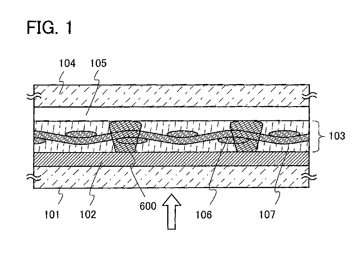
[0058]A photoelectric conversion device according to an embodiment of the present invention includes at least two cells. The cells each have a single-layer structure or a stack structure of a photoelectric conversion layer which is the minimum unit having a photoelectric conversion function. Further, the photoelectric conversion device has at least one structure body which is formed in such a manner that a fibrous body is impregnated with a resin and is interposed between the two cells. The structure of the photoelectric conversion device according to an embodiment of the present invention will be described with reference to FIG. 1.

[0059]A photoelectric conversion device illustrated in FIG. 1 includes a cell 102 (also referred to as a first cell) supported by a substrate 101 (also referred to as a first substrate), a structure body 103, and a cell 105 (also referred to as a second cell) supported by a substrate 104 (also referred to as a second substrate). The structure body 103 is ...

embodiment 2

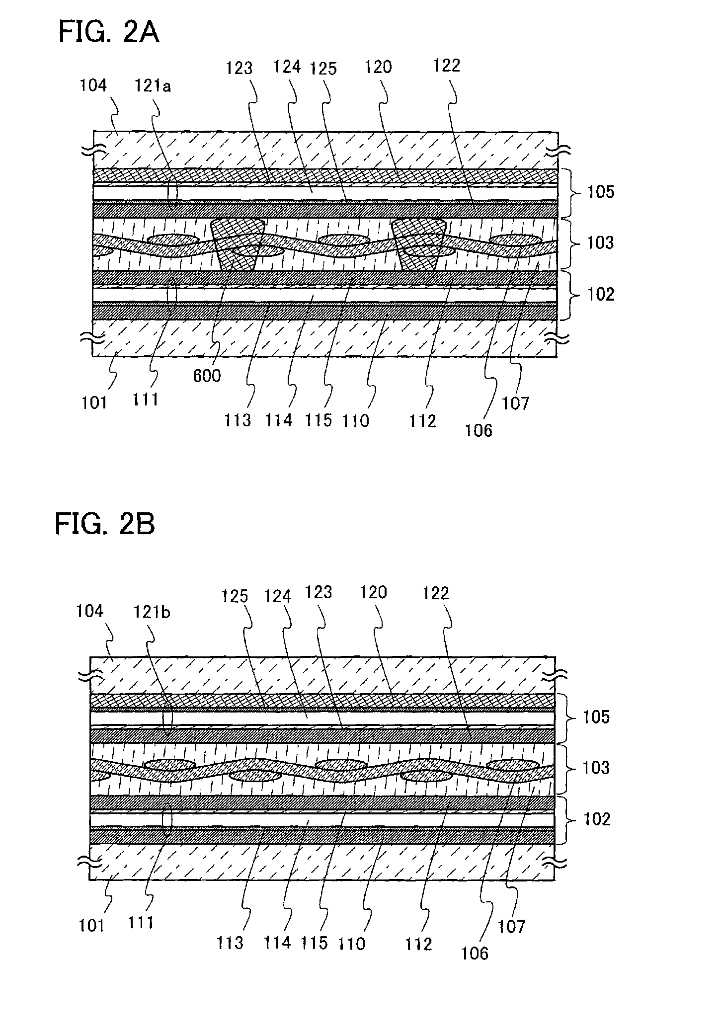
[0120]In this embodiment, a method for manufacturing a photoelectric conversion device of the invention disclosed herein will be described using the photoelectric conversion device illustrated in FIG. 2A as an example.

[0121]First, formation of the cell 102 over the substrate 101 will be described. As illustrated in FIG. 6A, the conductive film 110 which is patterned (processed in a predetermined shape) is formed over the substrate 101. In this embodiment, since the photoelectric conversion device in which light enters from the substrate 101 side is described as an example, it is preferable that the substrate 101 have a light-transmitting property with respect to visible light. For example, the substrate 101 can be formed using any of various commercial glass plates of soda-lime glass, opaque glass, lead glass, tempered glass, ceramic glass, and the like. Further, a non-alkali glass substrate of aluminosilicate glass, barium borosilicate glass, aluminoborosilicate glass, or the like;...

embodiment 3

[0168]In this embodiment, a structure in which a cell including a photoelectric conversion layer is formed over and attached to a plastic substrate (a flexible substrate) will be described. Specifically, an example of the following structure will be described. In the structure, after a layer to be separated including a photoelectric conversion layer is formed over a supporting substrate having high heat resistance such as a glass substrate or a ceramic substrate with a separation layer and an insulating layer interposed therebetween, the supporting substrate and the layer to be separated are separated from each other using the separation layer, and the layer to be separated which is separated is attached to a plastic substrate to form a cell over the plastic substrate. In this embodiment, fabrication of a cell which is placed on the side opposite to the light incident side (a bottom cell) will be described. When a cell formed by a manufacturing method described in this embodiment is...


PUM


Abstract

A multi junction photoelectric conversion device that can be manufactured by a simple method is provided. In addition, a photoelectric conversion device whose mechanical strength is increased without complicating a manufacturing process is provided. A photoelectric conversion device includes a first cell having a photoelectric conversion function, a second cell having a photoelectric conversion function, and a structure body including a fibrous body, which firmly attaches and electrically connects the first cell and the second cell to each other. Accordingly, a multi-junction photoelectric conversion device in which semiconductor junctions are connected in series and sufficient electrical connection between p-i-n junctions is ensured can be provided.

Description

TECHNICAL FIELD[0001]The present invention relates to a photoelectric conversion device which can generate electric energy from light and a method for manufacturing the photoelectric conversion device.BACKGROUND ART[0002]A solar cell is one kind of photoelectric conversion device which, using a photovoltaic effect, directly converts received light into electric power and outputs the electric power. Unlike a conventional power generation system, a power generation system using the solar cell does not need energy conversion to thermal energy or kinetic energy in the process. Therefore, although fuel is consumed when solar cells are produced or set, the solar cells have an advantage in that the amount of greenhouse gas typified by carbon dioxide or of emission gas containing a toxic substance per electric power generated is remarkably smaller than that of an energy source based on fossil fuel. In addition, the energy of light from the sun which reaches the earth for one hour correspond...

Claims


Application Information

Patent Timeline
IPC IPC(8): H01L31/042H01L31/18
CPCB60T1/10H01L31/03685H01L2924/0002H01L31/03926H01L31/048H01L31/0488H01L31/0687H01L31/076H01L2924/09701Y02E10/544Y02E10/545Y02E10/548Y02E10/549H01L31/043H01L2924/00Y02P70/50
Inventor YAMAZAKI, SHUNPEISUZUKI, YUKIENISHI, KAZUO
Owner SEMICON ENERGY LAB CO LTD
Why Eureka
Try Eureka