Photonic crystal band-shifting device for dynamic control of light transmission

a photonic crystal and light transmission technology, applied in the field of optical devices, can solve the problems of over 1 cm of total device length, inability to integrate on silicon substrates, and inability to use on-chip optical interconnects, etc., to achieve the effect of reducing power dissipation, reducing heating generation of optoelectronic devices, and improving modulator performan

Inactive Publication Date: 2010-12-09
OMEGA OPTICS
View PDF6 Cites 18 Cited by
  • Summary
  • Abstract
  • Description
  • Claims
  • Application Information

AI Technical Summary

Benefits of technology

[0009]Another object of the invention is to reduce the power dissipation and mitigate heating generation of the optoelectronic device.
[0010]The third object of the invention is to improve the modulator performance in terms of reducing optical loss by significantly shortening the total device length, especially by shortening the photonic crystal waveguide length.

Problems solved by technology

However, conventional telecom optical modulators using LiNbO3 or III-V semiconductor materials cannot be integrated on silicon substrates.
But the total device length is over 1 cm and is not suitable for on-chip optical interconnects. M. Lipson's group at Cornell University reported ultra-compact silicon ring-resonator modulators with 10 μm diameter (M. Lipson, “Compact electro-optic modulators on a silicon chip,” IEEE J. Sel. Topics in Quantum Electron., 12, 6, 1520-1526, 2006).
However, the total device length is still several millimeters when including the conventional splitting and merging waveguide.
Although an all-photonic-crystal approach can further reduce the total length, such a device is very lossy, especially in the slow photon region.

Method used


Image

  • Photonic crystal band-shifting device for dynamic control of light transmission
  • Photonic crystal band-shifting device for dynamic control of light transmission
  • Photonic crystal band-shifting device for dynamic control of light transmission

Examples


Embodiment Construction

[0027]Detailed descriptions of the preferred embodiments are provided herein. It is to be understood, however, that the present invention may be embodied in various forms. Therefore, specific details disclosed herein are not to be interpreted as limiting, but rather as a basis for the claims and as representative basis for teaching one skilled in the art to employ the present invention in virtually any appropriately detailed system, structure or manner.

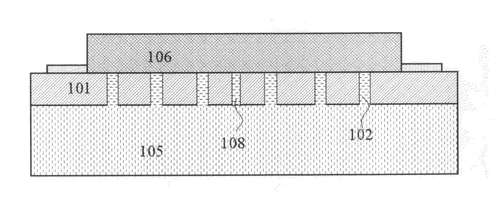
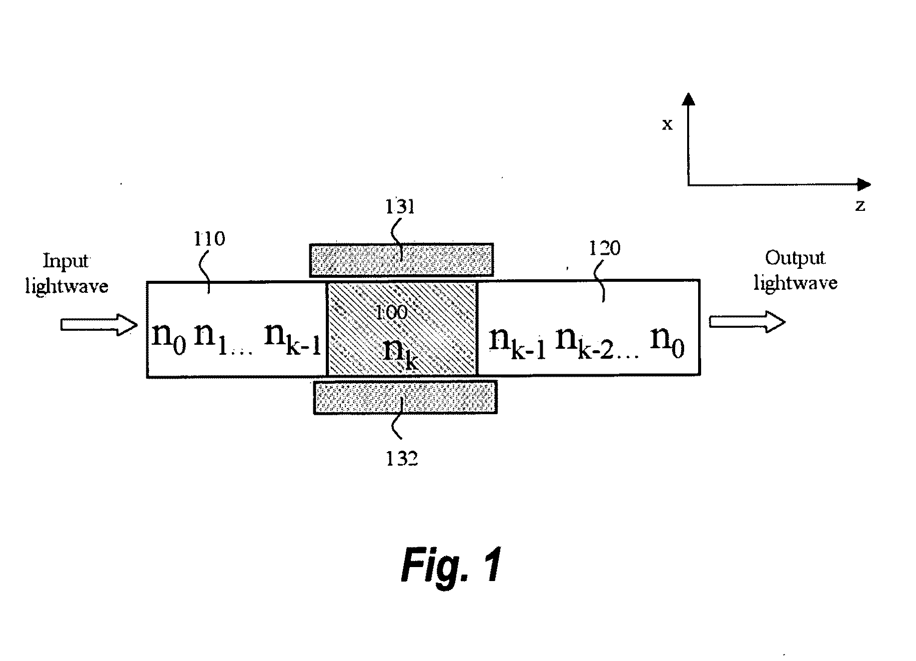
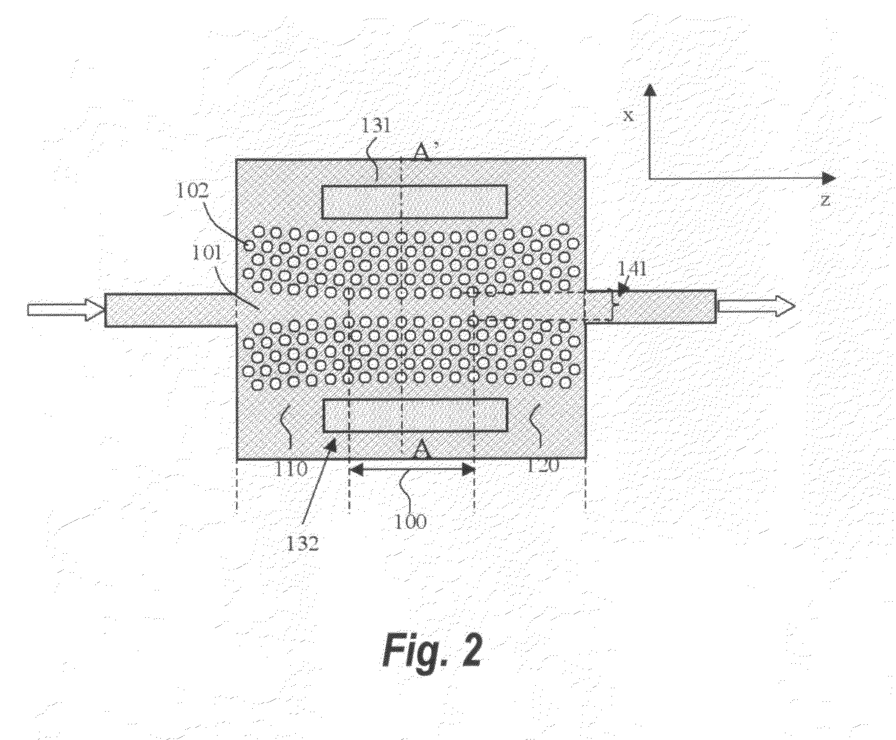
[0028]With increasing concerns about power consumption and electromagnetic interference (EMI) as the feature size of VLSI circuits pushes deeper and deeper into nanometer scale, using sub-micron photonic technology for chip-to-chip and on-chip communications becomes an essential solution for the stringent demands on bit rates and power dissipation. Monolithically integrated modulators, especially silicon electro-optic (E-O) modulators, will play a key role for on-chip and chip-to-chip optical interconnects. The present invention on ba...


PUM


Abstract

An active device for dynamic control of lightwave transmission properties has at least one photonic crystal waveguide that has anti-reflection photonic crystal waveguides with gradually changed group refractive indices at both input and output side. An alternating voltage or current signal applied to two electrically conductive regions changes the refractive indices of the photonic crystal materials, introducing a certain degree of blue-shift or red-shift of the transmission spectrum of the photonic crystal waveguide. The output lightwave with frequency close to the band-edge of the photonic crystal waveguide is controlled by the input electric signal. Devices having one or more such active photonic crystal waveguides may be utilized as an electro-optic modulator, an optical switch, or a tunable optical filter.

Description

STATEMENT REGARDING FEDERALLY SPONSORED RESEARCH[0001]The U.S. Government has a paid-up license in this invention and the right in limited circumstances to require the patent owner to license others on reasonable terms as provided for by the terms of the contracts FA9550-09-C-0086 awarded by Air Force Office of Scientific Research.BACKGROUND OF THE INVENTION[0002]1. Field of the Invention[0003]This invention relates generally to the field of optical devices, and more specifically to an apparatus and method for modulation, switching and dynamic control of light transmission using photonic crystals.[0004]2. Description of the Related Art[0005]On-chip optical modulators have paramount significance as inter- and intra-chip optical interconnects become an essential solution to the great challenges in speed, power dissipation and electromagnetic interference (EMI) that modern very large scale circuitry (VLSI) technology is facing. On-chip optical modulators, especially monolithically inte...

Claims


Application Information

Patent Timeline
Patent Type & Authority Applications(United States)
IPC IPC(8): G02B6/12G02B6/10G02B6/26
CPCB82Y20/00G02B6/1225G02F2202/32G02F1/035G02F1/025
Inventor WANG, XIAOLONGCHEN, RAY T.
Owner OMEGA OPTICS
Why Eureka
Try Eureka