Functional Integration Of Dilute Nitrides Into High Efficiency III-V Solar Cells

Inactive Publication Date: 2010-12-23
ARRAY PHOTONICS INC
View PDF92 Cites 51 Cited by
  • Summary
  • Abstract
  • Description
  • Claims
  • Application Information

AI Technical Summary

Benefits of technology

[0030]According to the invention, in a multi junction solar cell composed of III-V materials, including a dilute nitride subcell, additional layers of material effecting mid-gap states are inserted into one or more of the tunnel junctions in a manner to achieve a tunnel junction design that is thermally stable and exhibits good performance after extraordinary thermal annealing times and temperatures required by the dilute nitride material in the solar cell. An appropriate thermal energy dose or loading can be effected in an number of ways such as by heating the entire structure, and it may include adding an additional thermal step

Problems solved by technology

However, the integration of dilute nitride materials into a solar cell requires more than lattice matching.
To date, it has not been shown how to solve these integration problems to create a high performance dilute nitride sub-cell in a multi-junction solar cell without destroying the performance of other sub-cells, sub-structures, or the solar cell as a whole.
These defects can both harm device performance and device reliability.
Despite its predicted benefits to solar cell efficiency, dilute nitrides are not used in commercial III-V solar cells because producing dilute nitride sub-cells with the proper band gap that also produce currents high enough to achieve current matching has been extremely challenging.
Generally, the temperatures and times used for additional growth on top of the dilute nitride layer are not sufficient to improve the parameters of the dilute nitride to the fullest extent.
It is not enough to make a good stand-alone dilute nitride sub-cell.
While beneficial to the GaInNAs sub-cell, the application of the thermal load (or dose) to the dilute nitride sub-cell (or cells) may adversely affect the other sub-structures dramatically.
One can clearly see that the wafer which got the hotter anneal exhibits a clear tunnel junction failure.
However, it is difficult to achieve n-type doping above about 5e18 cm−3 with the standard silicon dopant.
It is particularly difficult to maintain activated doping levels above 5e18 cm−3 Silicon post anneal.
Likewise, when beryllium is u

Method used


Image

  • Functional Integration Of Dilute Nitrides Into High Efficiency III-V Solar Cells
  • Functional Integration Of Dilute Nitrides Into High Efficiency III-V Solar Cells
  • Functional Integration Of Dilute Nitrides Into High Efficiency III-V Solar Cells

Examples


Embodiment Construction

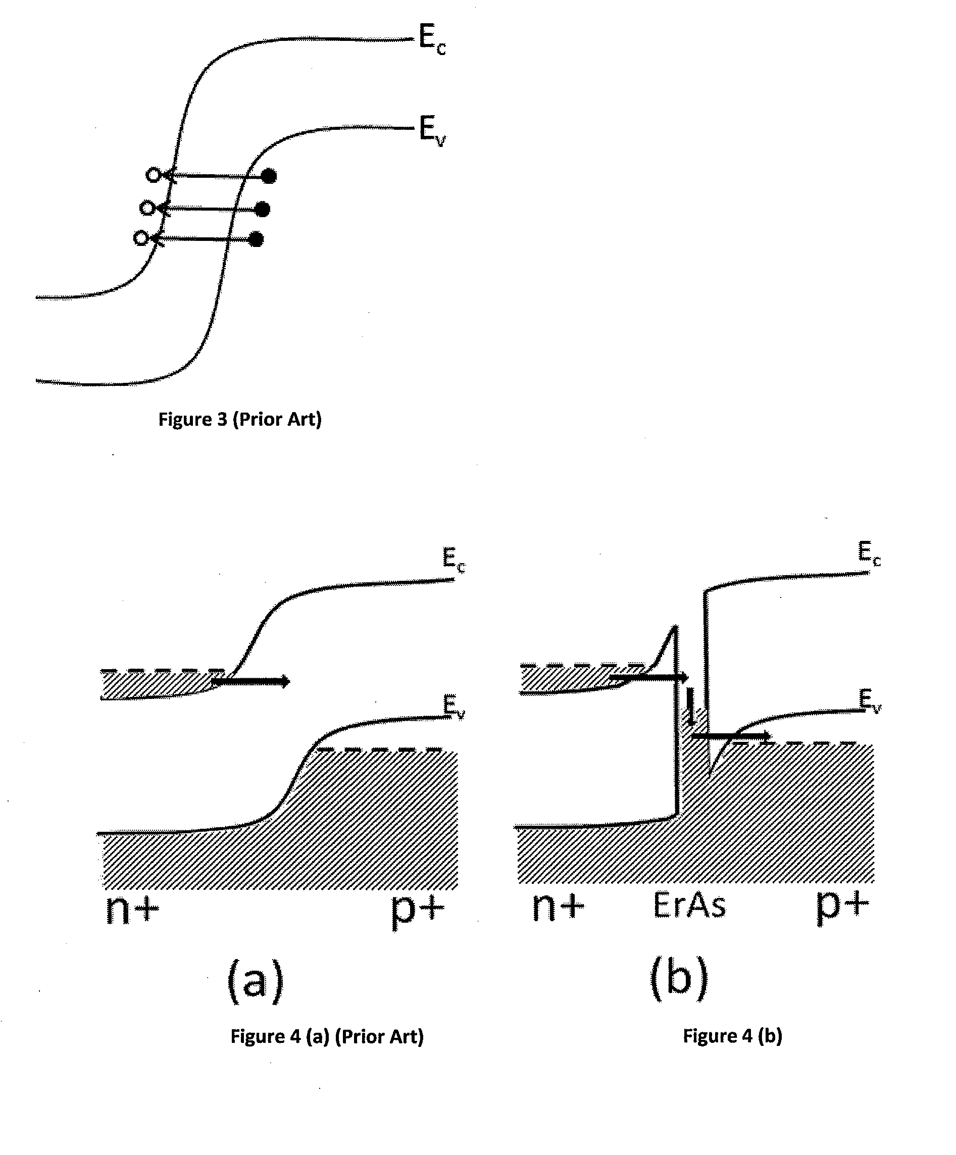
[0042]Referring to FIG. 4(b), the operation of a tunnel junction with erbium arsenide is illustrated. The operation comprises, first, the tunneling of electronic carriers from the higher potential n+ state of a III-V material into a thin interlayer of rare earth-Group V material, particularly erbium arsenide (ErAs), then second, the tunneling of electrons from the mid potential of the rare-earth-Group V material into the lower potential p+ state of a III-V material, such as gallium arsenide (GaAs).

[0043]Thus electronic carriers have only to tunnel through a small barrier into the mid-gap state, then through a small barrier out of the mid-gap state. This reduction in tunnel barrier magnitude increases the tunnel current for a given applied bias. (See FIG. 5, dashed curve 1). The lowering of the tunnel barrier magnitude is also useful when making tunnel junctions out of higher band gap materials.

[0044]For a desired current level through a tunnel junction incorporating mid-gap states (...


PUM


Abstract

Tunnel junctions are improved by providing a rare earth-Group V interlayer such as erbium arsenide (ErAs) to yield a mid-gap state-assisted tunnel diode structure. Such tunnel junctions survive thermal energy conditions (time/temperature) in the range required for dilute nitride material integration into III-V multi-junction solar cells.

Description

CROSS-REFERENCES TO RELATED APPLICATIONS[0001]Not ApplicableSTATEMENT AS TO RIGHTS TO INVENTIONS MADE UNDER FEDERALLY SPONSORED RESEARCH AND DEVELOPMENT[0002]Not ApplicableREFERENCE TO A “SEQUENCE LISTING,” A TABLE, OR A COMPUTER PROGRAM LISTING APPENDIX SUBMITTED ON A COMPACT DISK[0003]Not ApplicableBACKGROUND OF THE INVENTION[0004]This invention relates to photo-voltaic solar cell technology and in particular to the process for constructing high efficiency multi junction III-V solar cells.[0005]A III-V solar cell is formed by integrating various sub-cells together in a single layered structure into a single functioning solar cell. Each of the sub-cells absorbs light in different regions of the solar spectrum and convert that light into current and voltage. These sub-cells are electrically connected by sub-structures called tunnel junctions. Each of these sub-structures impacts the overall performance of the solar cell, and integration is not trivial. For example, in a conventional...

Claims


Application Information

Patent Timeline
IPC IPC(8): H01L31/0304H01L31/18
CPCH01L31/03042Y02E10/544H01L31/0687H01L31/03048H01L31/035209
Inventor WIEMER, MICHAEL W.YUEN, HOMAN B.SABNIS, VIJIT A.SHELDON, MICHAEL J.FUSHMAN, ILYA
Owner ARRAY PHOTONICS INC
Why Eureka
Try Eureka