Liquid crystal display device

a liquid crystal display and display device technology, applied in optics, instruments, optical elements, etc., can solve problems such as increasing power consumption, achieve the effects of enhancing the intensity of blue transmitted light, reducing power consumption, and increasing the effective display area

Active Publication Date: 2010-12-23
PANASONIC LIQUID CRYSTAL DISPLAY CO LTD +1
View PDF7 Cites 29 Cited by
  • Summary
  • Abstract
  • Description
  • Claims
  • Application Information

AI Technical Summary

Benefits of technology

[0044]Instead of giving equal areas to the three primary colors, blue, green, and red, blue pixels may be given a higher ratio of effective display area than green pixels or red pixels. Using this structure in which the area ratio of blue pixels is raised is effective in enhancing the intensity of blue transmitted light.
[0045]When the above-mentioned structure is modified such that green pixels are given a larger effective display area than red pixels, the luminous transmittance is prevented from dropping and a light source having a strong tone of red which is very high in light emission efficiency can be used, with the result that the power consumption of the light source is reduced. Reducing the power consumption of the light source has a great effect on a reduction in overall power consumption of the system because most of the power consumption of a liquid crystal display device is attributed to the light source.
[0046]Structured as described above, a liquid crystal display device is improved in light utilization efficiency in the short-wavelength range which has conventionally been an issue. This provides the liquid crystal display device such effects as less power consumption necessary for the light source, prevention of color tone changes in white display and black display, and prevention of color unevenness which is caused by fluctuations in intensity of blue light.
[0047]The power consumption can be reduced because, as described above, the above-mentioned structure enables setting the color temperature of the light source low. Color tone changes in white display and black display, too, are caused by the loss of short-wavelength range light in white display and pose a problem in displaying a high-quality image. When the loss of short-wavelength light in white display is large, the color temperature of the light source is high and the intensity is high in the short-wavelength range. Light in black display, on the other hand, is not usually expected transmitted light and is rather an defect of light-shielding performance of the liquid crystal display device. This is mai...

Problems solved by technology

This means that the luminance of the light source has to be considerably high in order to achieve a satisfactorily high white luminance, in particular, 500 nits w...

Method used


Image

  • Liquid crystal display device
  • Liquid crystal display device
  • Liquid crystal display device

Examples


embodiment 1

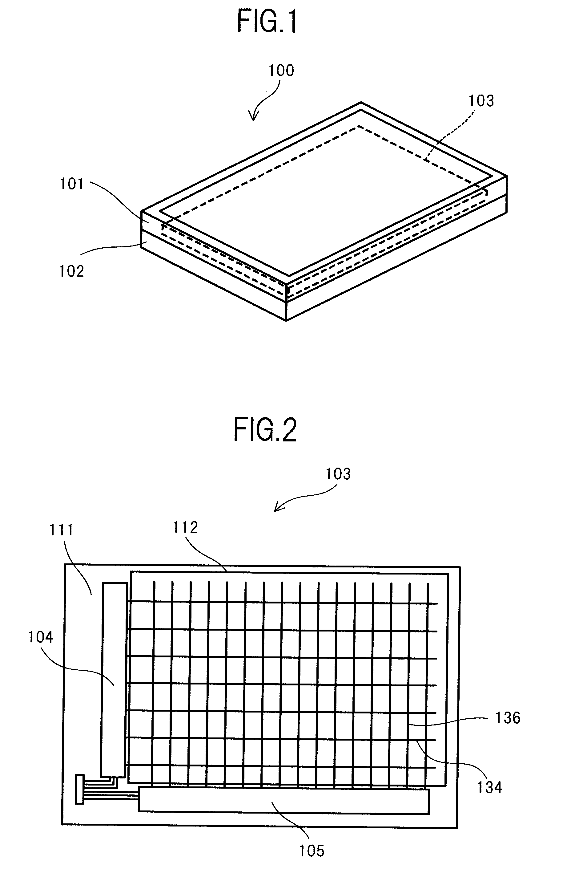
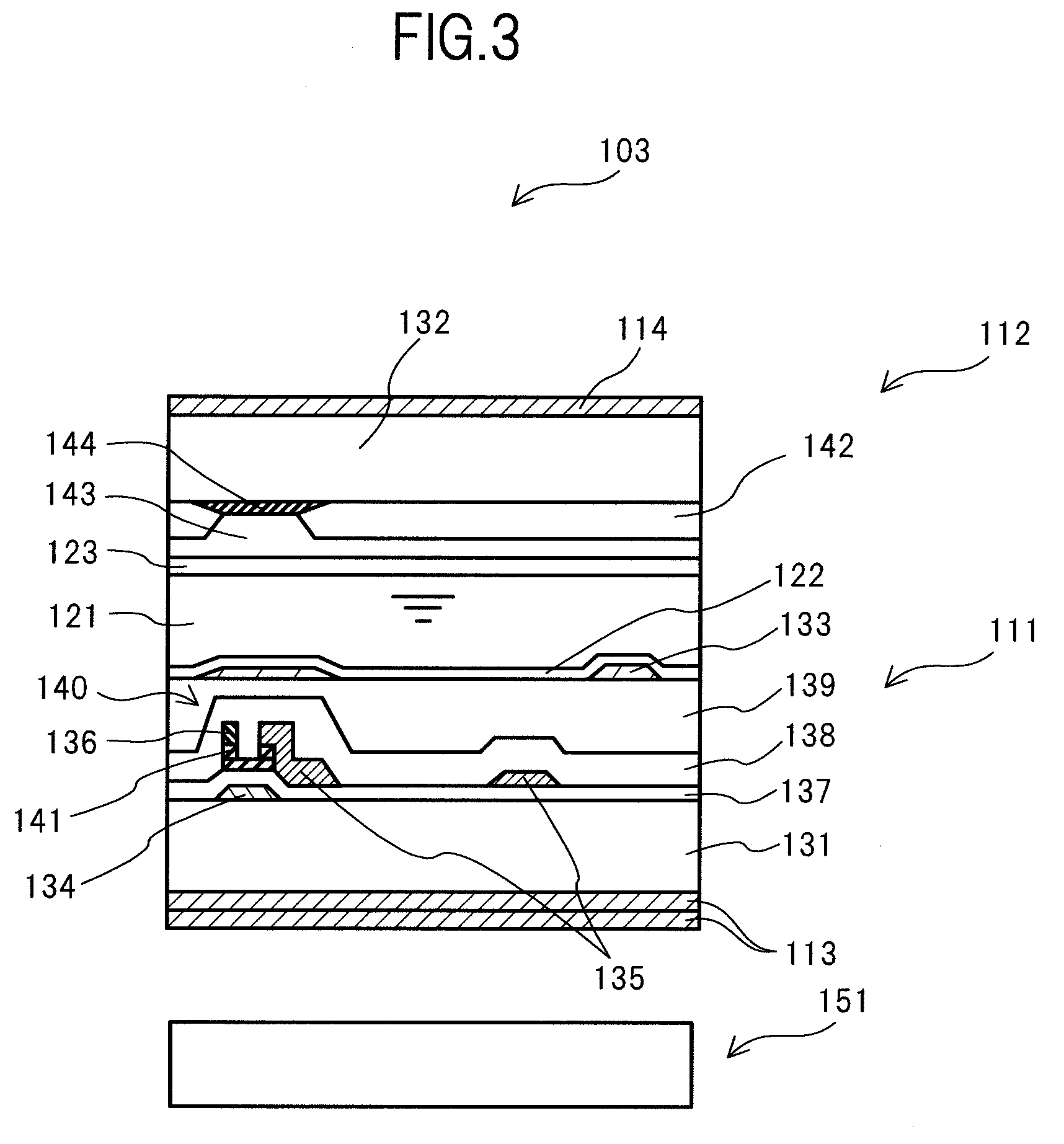
[0072]FIG. 1 schematically illustrates a liquid crystal display device 100 according to an embodiment mode of the present invention. As illustrated in FIG. 1, the liquid crystal display device 100 includes a liquid crystal display panel 103, which is fixed to be sandwiched between an upper frame 101 and a lower frame 102, a backlight unit (not shown), and other components.

[0073]FIG. 2 illustrates the structure of the liquid crystal display panel 103. The liquid crystal display panel 103 includes two substrates, an active matrix substrate 111 and a color filter substrate 112, between which a liquid crystal 121 is sealed. Scanning electrodes 134, which are controlled by a driver circuit 104, and signal electrodes 136, which are controlled by a driver circuit 105, run all over the active matrix substrate 111. These signal lines intersect each other to form pixels of the liquid crystal display device 100. The liquid crystal display panel 103 includes a number of pixels that corresponds ...

embodiment 2

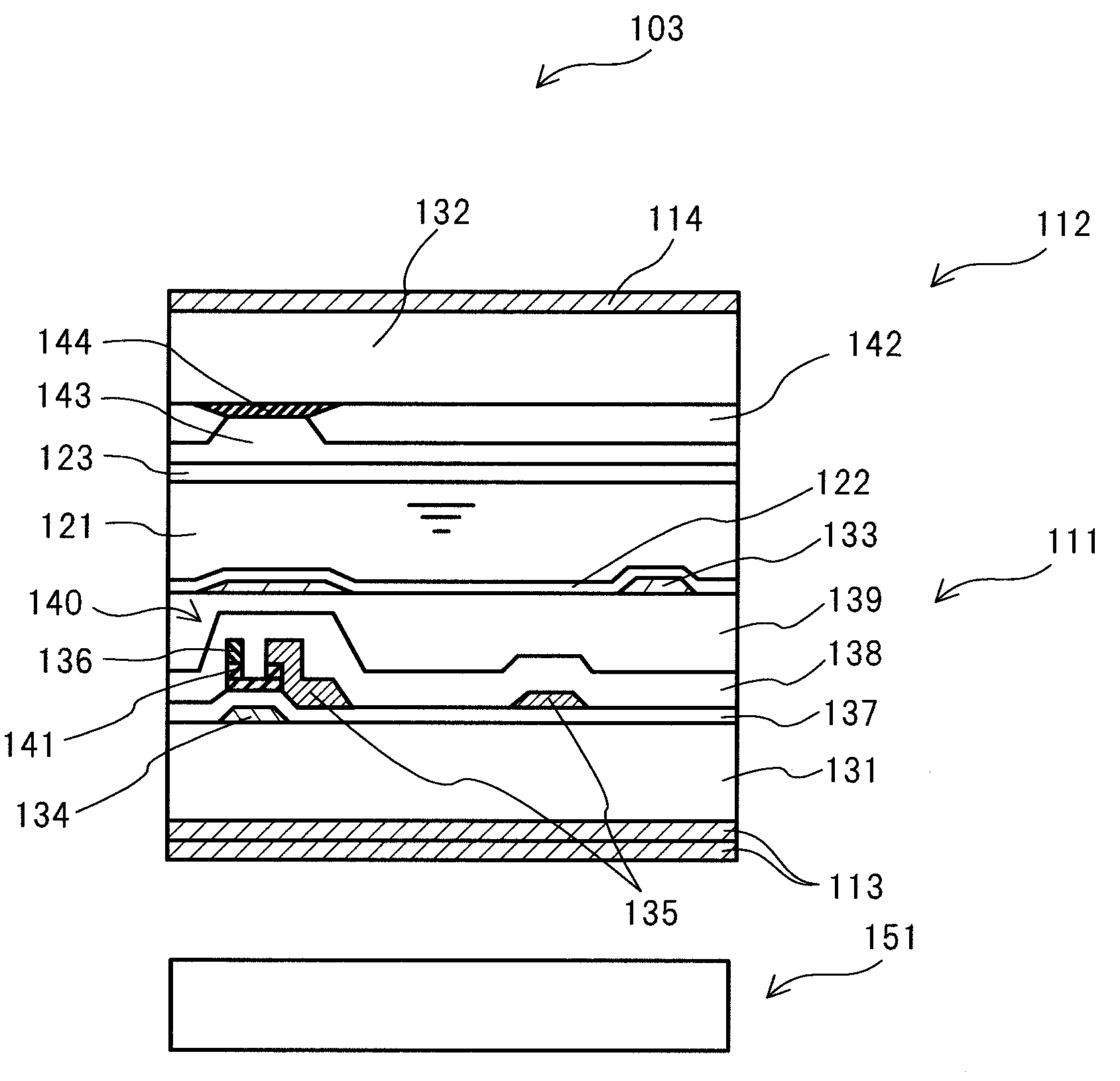
[0105]FIG. 8 is a schematic sectional view of one pixel and its vicinities in the display panel 203 of the liquid crystal display device 200 according to the present invention. The exterior structure of the liquid crystal display device 200 and the display panel 203 is the same as the one described in Embodiment 1 with reference to FIGS. 1 and 2, and hence the description is not repeated here.

[0106](Active Matrix Substrate)

[0107]FIG. 9 is a schematic diagram of one pixel and its vicinities on an active matrix substrate 211 of the display panel 203 according to the present invention. FIG. 10 is an enlarged sectional view of a thin-film transistor and its vicinities on the active matrix substrate.

[0108]As illustrated in FIG. 10, a common electrode 233 made of indium-tin-oxide (ITO), a scanning electrode 234 made of molybdenum / aluminum (Mo / Al), and a common electrode wiring line (common wiring line) 246 are formed on a glass substrate 231 of the active matrix substrate 211. The common ...

embodiment 3

[0129]FIG. 14 is a schematic sectional view of one pixel and its vicinities in a display panel 303 of a liquid crystal display device 300 according to the present invention. The exterior structure of the liquid crystal display device 300 and the display panel 303 is the same as the one described in Embodiment 1 with reference to FIGS. 1 and 2, and hence the description is not repeated here. In Embodiment 3, components identical or similar to those in Embodiment 2 are denoted by the same reference symbols in order to omit their descriptions.

[0130](Color Filter Substrate)

[0131]In a color filter substrate 342 of Embodiment 3, a blue filter, a green filter, and a red filter have an area ratio of 1.09:1:0.85.

[0132](Color Filter Substrate-Side Alignment Film)

[0133]A color filter substrate-side alignment film 323 is formed as follows. As monomer components, diamine is prepared by mixing 4,4′-diaminoazobenzene and 4,4′-diaminobenzophenone at a molar ratio of 6:4, and an acid anhydride is pr...


PUM


Abstract

A liquid crystal display device includes: a liquid crystal layer which contains a liquid crystal composition; a pair of substrates opposed to each other across the liquid crystal layer; alignment layers placed on liquid crystal layer sides of the pair of substrates, respectively; and polarization plates placed on opposite sides from the liquid crystal layer sides, respectively. The pair of substrates includes a thin-film transistor substrate including a thin-film transistor for controlling molecule alignment of the liquid crystal composition, and a color filter substrate including a color layer containing pixels of different colors. A blue pixel, which is one of the pixels of different colors, is larger in area than any of the pixels of other colors. A loss of light in a short-wavelength range is thus reduced.

Description

CROSS-REFERENCE TO RELATED APPLICATION[0001]The present application claims priority from Japanese application JP 2009-147762 filed on Jun. 22, 2009, the content of which is hereby incorporated by reference into this application.BACKGROUND OF THE INVENTION[0002]1. Field of the Invention[0003]The present invention relates to a liquid crystal display device.[0004]2. Description of the Related Art[0005]With advance of technology for improving image quality of liquid crystal displays and with advantage of being less thick and more lightweight than a cathode ray tube (CRT, also generally referred to as “Braun tube”) which had been a mainstream of display devices, use and market for the liquid crystal displays have been expanding.[0006]In recent years, electric appliances are expected to be low in power consumption in order to suppress the used amount of fossil fuel for protecting the global environment, especially as an anti-global warming measure. In transmissive liquid crystal display d...

Claims


Application Information

Patent Timeline
IPC IPC(8): G02F1/1335G02F1/13357
CPCG02F1/133514G02F1/134363G02B5/3008G02B5/223G02F2201/52
Inventor UTSUMI, YUKATOMIOKA, YASUSHIHIYAMA, IKUO
Owner PANASONIC LIQUID CRYSTAL DISPLAY CO LTD
Why Eureka
Try Eureka