
Optical Devices Having Controlled Nonlinearity

a technology of optical devices and nonlinearities, applied in the field of optical devices, can solve the problems of increasing the characteristic quality factor of the device, and reducing the performance of the device, so as to achieve the effect of improving the device performan

Inactive Publication Date: 2011-01-06
MASSACHUSETTS INST OF TECH
View PDF18 Cites 14 Cited by
  • Summary
  • Abstract
  • Description
  • Claims
  • Application Information

AI Technical Summary

Benefits of technology

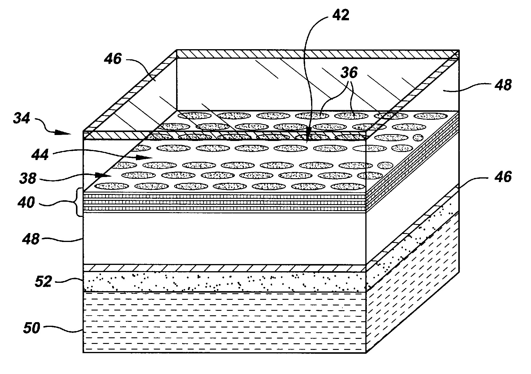
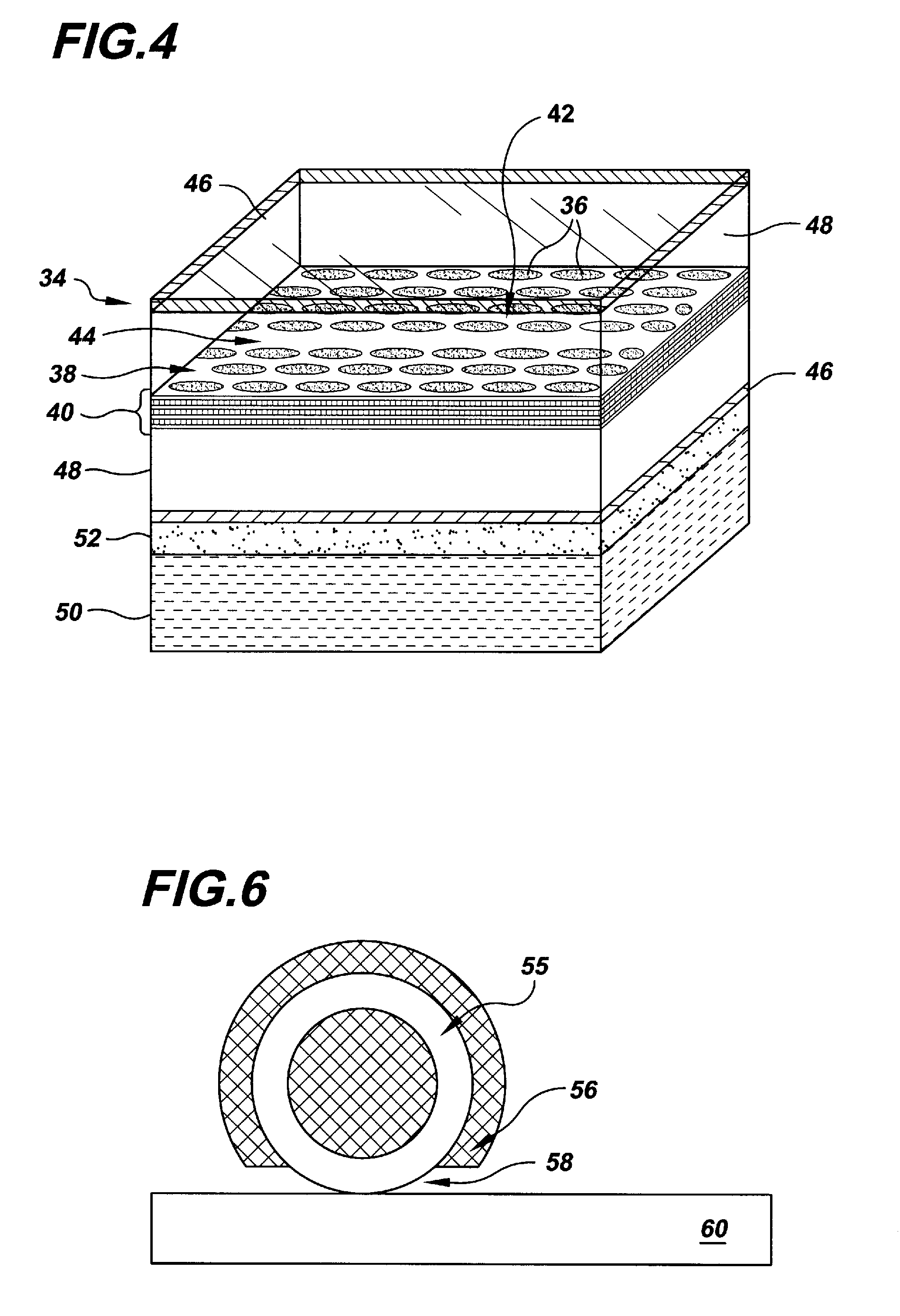
The invention provides optical device designs that control the nonlinearity of the device to enhance its performance. The device includes a solid state nonlinear material with a nanostructured extent and an electronic band gap at least twice as large as the energy of a photon. The nonlinear material has a switching figure of merit at least about 2π. A dielectric structure is provided around the nonlinear material with a characteristic photonic band gap that overlaps the electronic band gap. A waveguide is provided in proximity to the nonlinear material for coupling light to it. The device arrangement enables a wide range of optical device operations and configurations with operational capabilities not previously attainable. It allows for all-optical signal processing devices with operating powers and switching times orders of magnitude smaller than traditional nonlinear optical devices.

Problems solved by technology

In general, optical nonlinearities are typically quite weak in an optical material.
But many optical processing operations and optical devices cannot operate fully as-intended without a relatively strong nonlinearity.
But although this approach does enhance nonlinearity, it typically also increases the characteristic quality factor of the device, which in turn decreases, e.g., the switching speed of the device.
But in general, highly nonlinear materials are characterized by other properties that are deleterious for optical processing.
For example, many highly nonlinear materials are also characterized by a degree of optical absorption that is prohibitively high for many optical processing applications.

Method used


Image

  • Optical Devices Having Controlled Nonlinearity
  • Optical Devices Having Controlled Nonlinearity
  • Optical Devices Having Controlled Nonlinearity

Examples


first example class

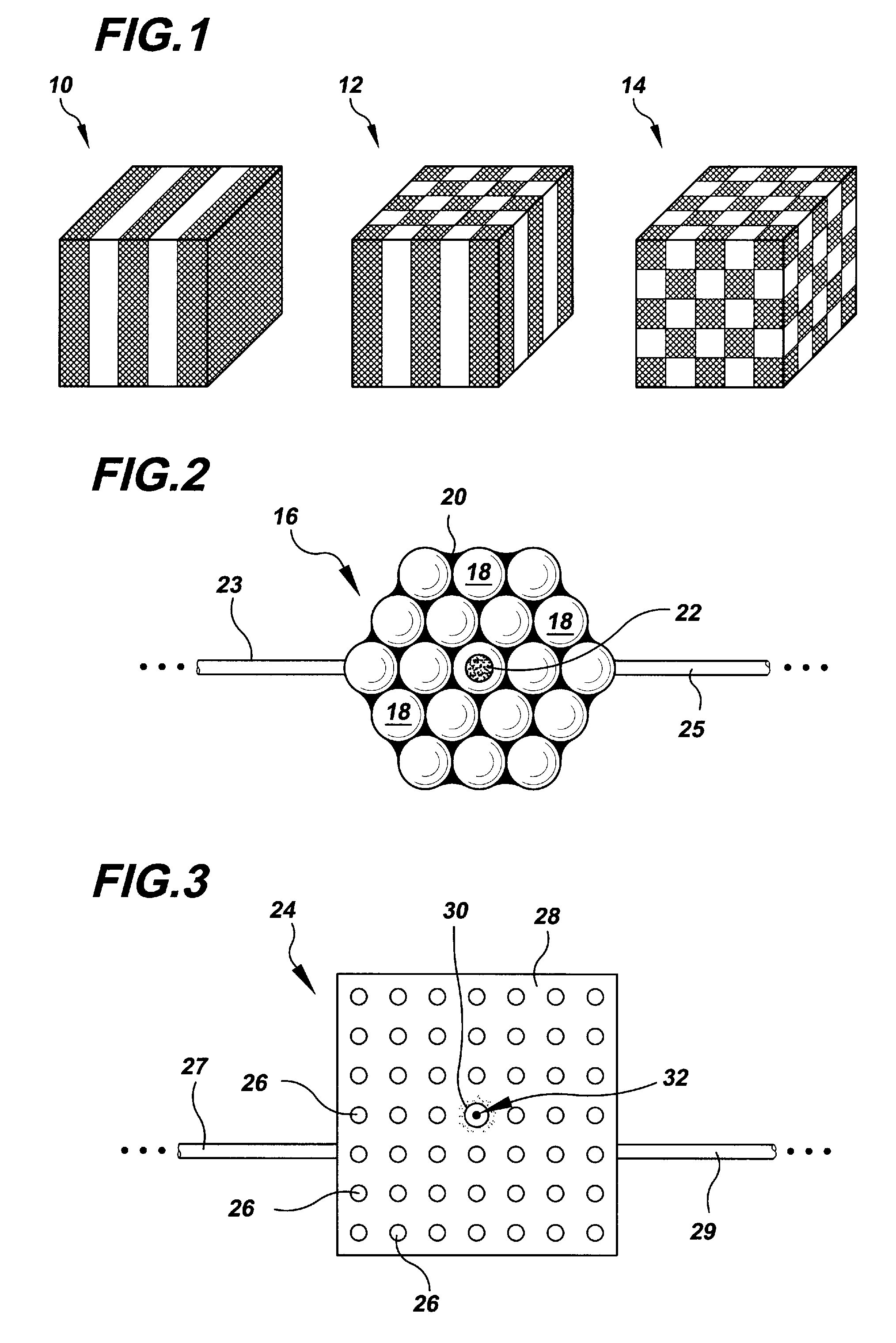
dielectric environments to be employed in accordance with the invention is the class of photonic crystals. A photonic crystal is a dielectric structure having a periodic, i.e., repeating, arrangement of alternating high-dielectric and low-dielectric regions. With sufficient index contrast and appropriate lattice structure, e.g., face-centered cubic arrangement of dielectric regions, a photonic band gap is produced in the photonic crystal. Propagation of light through the crystal within the photonic band gap is exponentially suppressed; in other words, a range of frequencies of light cannot propagate through the crystal, and that prohibited frequency range is characterized by the photonic band gap.

Conventionally, the periodicity of a photonic crystal lattice and the dimensions of the dielectric regions in the lattice are selected to suppress the propagation in the crystal of a selected incident wavelength for a given optical application. In accordance with the invention, the periodic...

example 1

The two-dimensional photonic crystal structure of FIG. 2 is analyzed for a two-dimensional triangular lattice of air holes in a dielectric medium of doped Si (ε=13). The nonlinear material provided at the center of the structure is provided as a GaAs—AlGaAs single quantum well. The periodicity of the photonic crystal is 331 nm, and the radius of the air holes is 158 nm.

FIG. 7A is a plot of the relative enhancement of the TM local density of states for the structure, as-measured in the time-domain simulation rate of emission, Γ, normalized by the emission rate in vacuum, Γo. Inside the photonic band gap of the structure, there is substantial but slightly incomplete suppression of emission. Outside the band gap, there is an enhancement of spontaneous emission because the density of states of the nonlinear material is shifted to frequencies surrounding the band gap. For an atom polarized in the direction out of the two-dimensional plane of the crystal, only the TM polarization need be ...

example 2

The two-dimensional photonic crystal structure of FIG. 3 is analyzed for a 7×7 square lattice of dielectric rods of Si, having ε=12.25, with a radius of 0.25α, where α is the period of the lattice. The rods are surrounded by air. The middle defect site is provided with a radius of 0.35α. A nonlinear material, namely, a CdSe nanocrystal, is provided at the defect site.

FIG. 8A is a plot of a numerical calculation of the enhancement of spontaneous emission for the structure, given as the ratio of the rate of emission of the nonlinear material in the photonic crystal, T1, purcell−1, divided by the emission rate in vacuum, T1,vac−1, as a function of frequency.

Given a value of T2≈0.13 fs at room temperature for a CdSe nanocrystal at the defect site, there is determined the enhancement, η, of the real part of the Kerr nonlinear susceptibility, χ(3), in the structure of FIG. 3, as a function of electronic transition frequency, ωelec, when probed at a frequency, ωph=0.508(2πc / a), the cavity'...


PUM

PropertyMeasurementUnit
temperatureaaaaaaaaaa
electronic band gapaaaaaaaaaa
speedaaaaaaaaaa

Abstract

An optical device is provided having a solid state nonlinear material with a nanostructured extent, in at least one dimension, that is less than about 10 nm or that is at a temperature of less than about 77 K. An electronic band gap, EGap, of the material is at least about twice as large as an energy of a photon with a wavelength, λ, equal to an operational wavelength of the device. The material is characterized by a switching figure of merit, ξ, having a value that is at least about 2π. A dielectric structure is around at least one dimension of the nonlinear material in a geometric arrangement having a characteristic photonic band gap that at least partially overlaps the electronic band gap of the material. At least one waveguide is disposed at the dielectric structure in sufficient proximity with the material for coupling light to the material.

Description

BACKGROUND OF INVENTIONThis invention relates generally to optical devices, and more particularly relates to optical device nonlinearities.An optical material can be characterized by its optical nonlinearity, which relates the nonlinear dependence of the polarization of the material to the optical field strength in the material. For example, the Kerr nonlinearity is distinguished by an index of refraction that depends linearly on the intensity of light present in the nonlinear material. Such a nonlinearity, and optical nonlinearities in general, enable a range of important optical phenomena, including frequency mixing, supercontinuum generation, and soliton propagation. Optical signal processing, such as higher-harmonic generation, and optical devices, such as optical switches, are fundamentally enabled by optical nonlinearities. For example, refractive index changes can be used to change the transmission characteristics of resonant cavities and other structures by modifying the eff...

Claims


Application Information

Patent Timeline
Patent Type & Authority Applications(United States)
IPC IPC(8): G02F1/035G02B6/00G02B6/26
CPCB82Y20/00G02B6/1225G02F1/035G02F2202/32G02F2001/01783G02F2202/101G02F1/3556G02F1/01783
Inventor BERMEL, PETERRODRIGUEZ, ALEJANDROSOLJACIC, MARINJOANNOPOULOS, JOHN
Owner MASSACHUSETTS INST OF TECH
Learn More