Process for producing indium oxide-type transparent electroconductive film

a technology of transparent electroconductive film and indium oxide, which is applied in the direction of vacuum evaporation coating, coating, semiconductor devices, etc., can solve the problems of difficult depositing such a transparent conductive film in an amorphous state, film exhibits a lower transparency than that of ito film, and the resistance of the film tends to increase, so as to achieve easy patterned with a weak acid

Inactive Publication Date: 2011-01-20
MITSUI MINING & SMELTING CO LTD
View PDF3 Cites 9 Cited by
  • Summary
  • Abstract
  • Description
  • Claims
  • Application Information

AI Technical Summary

Benefits of technology

[0031]According to the present invention employing a film Containing indium oxide and an additive element, there can be realized a transparent conductive film having such a composition that an amorphous film can be deposited at a predetermined film deposition temperature, and the produced amorphous film can be crystallized through annealing at a predetermined annealing temperature, and such that an optimum oxygen partial pressure at which the amorphous film deposited at the predetermined film deposition temperature has the lowest resistivity differs from an oxygen partial pressure at which a crystallized film obtained through annealing at the predetermined annealing temperature has the lowest resistivity. That is, the present invention produces a low-resistance transparent conductive film easily obtained through crystallization from an amorphous film which can be easily patterned with a weak acid.

Problems solved by technology

However, difficulty is encountered in depositing such a transparent conductive film in an amorphous state.
Meanwhile, indium oxide-zinc oxide (IZO) transparent conductive film, which is known as an amorphous film, poses a problem in that the film exhibits a transparency lower than that of ITO film and tends to be problematically yellowed.
However, when silicon is added to a transparent conductive film, resistance of the film tends to increase, which is problematic.
However, none of these patent documents describes, for example, an amorphous film or crystallization of an amorphous film.

Method used


Image

  • Process for producing indium oxide-type transparent electroconductive film
  • Process for producing indium oxide-type transparent electroconductive film
  • Process for producing indium oxide-type transparent electroconductive film

Examples


example 1

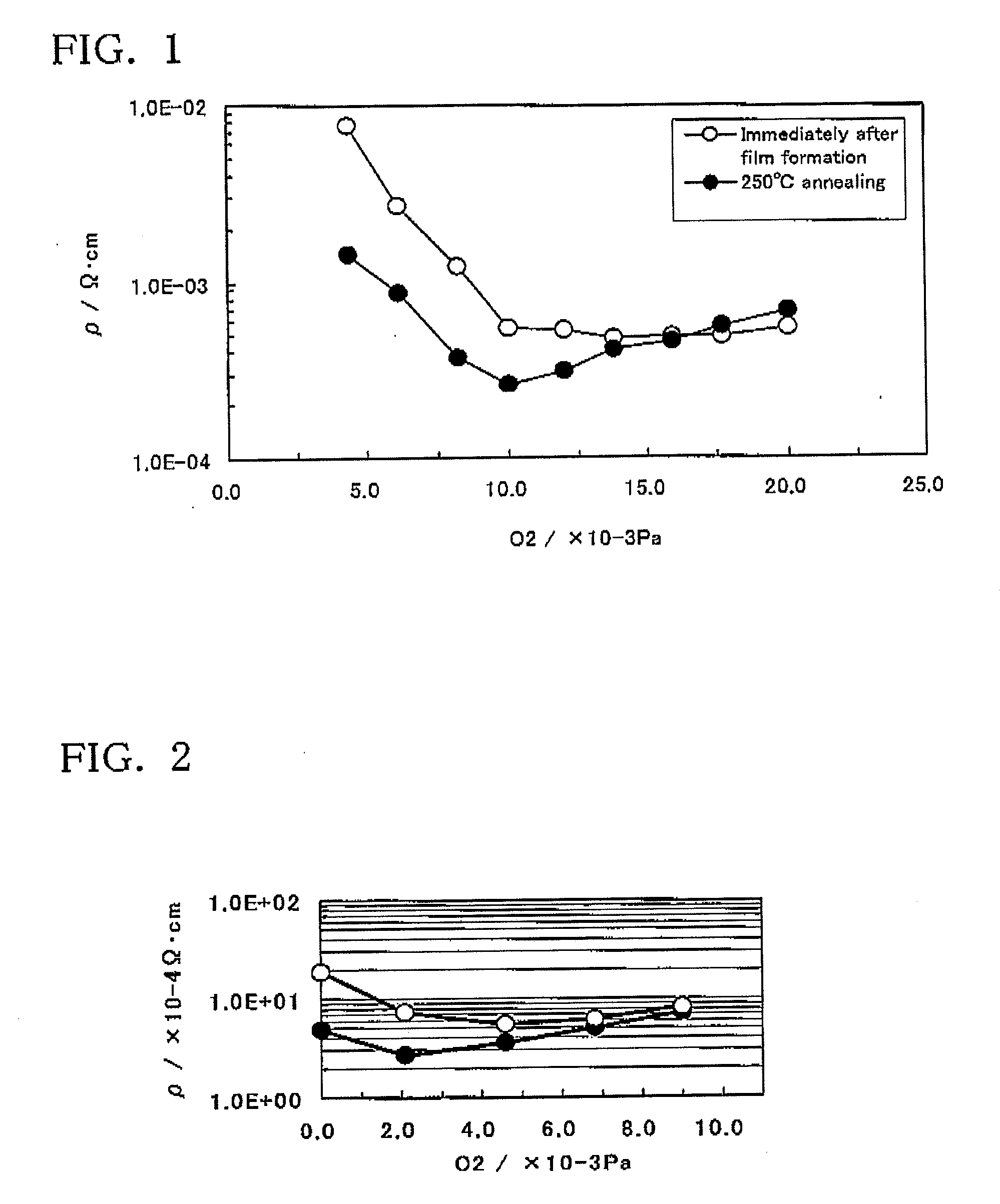
[0081]A >99.99%-purity In2O3 powder, a >99.99%-purity SnO2 powder, and a >99.9%-purity SiO2 powder were provided. These powders (total: about 2.5 Kg) were provided so that Si and Sn were respectively about 0.026 mol and 0.1 mol on the basis of 1 mol of In. The powders were formed into a compact through a filtration molding method. Thereafter, the compact was fired in an oxygen atmosphere at 1,550° C. for eight hours, to thereby produce a sintered compact. The sintered compact was processed, to thereby produce a target having a density of 7.01 g / cm3 (relative density of 100% with respect to the theoretical density). The target was found to exhibit a bulk resistivity of 2.4×10⁻⁴ Ω·cm.

[0082]While the oxygen partial pressure was varied from 0 to 4.0 sccm (corresponding to 0 to 2.0×10⁻² Pa), a film (thickness: 1,200 Å) was deposited from the thus-obtained target through DC magnetron sputtering under the following conditions.

Target dimensions: φ=8 inches, t=6 mm

Mode of sputtering: DC magn...
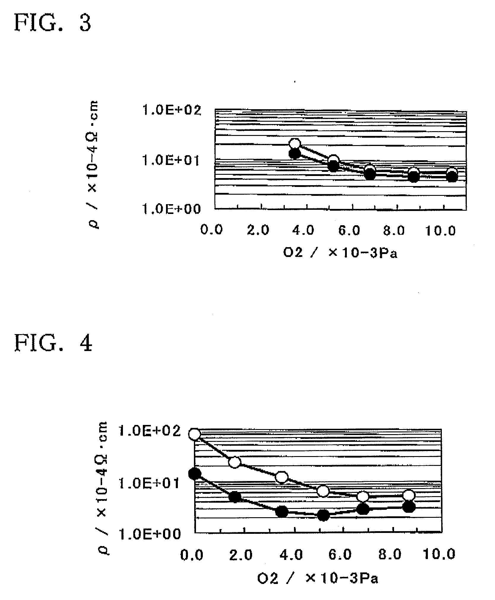
examples 2 and 3

[0086]A >99.99%-purity In2O3 powder, a >99.99%-purity SnO2 powder, and a >99.9%-purity BaCO3 powder were provided.

[0087]Firstly, In2O3 powder (BET=27 m2 / g) (58.5 wt. %) and BaCO3 powder (BET=1.3 m2 / g) (41.4 wt. %) (total: 200 g) were mixed by means of a ball mill in a dry state, and the mixture was calcined in air at 1,100° C. for three hours, to thereby yield BaIn2O4 powder.

[0088]Subsequently, the above-obtained BaIn2O4 powder, In2O3 powder (BET=5 m2 / g), and SnO2 powder (BET=1.5 m2 / g) (total: about 1.0 kg) were provided so that Ba and Sn were respectively 0.02 mol and 0.1 mol on the basis of 1 mol of In (Example 2), or so that Ba and Sn were respectively 0.005 mol and 0.3 mol on the basis of 1 mol of In (Example 3). These powders were mixed by means of a ball mill. Subsequently, the mixture was mixed with an aqueous PVA solution serving as a binder, dried, and cold-pressed, to thereby prepare a compact. The compact was debindered in air at 600° C. for 10 hours with temperature elev...
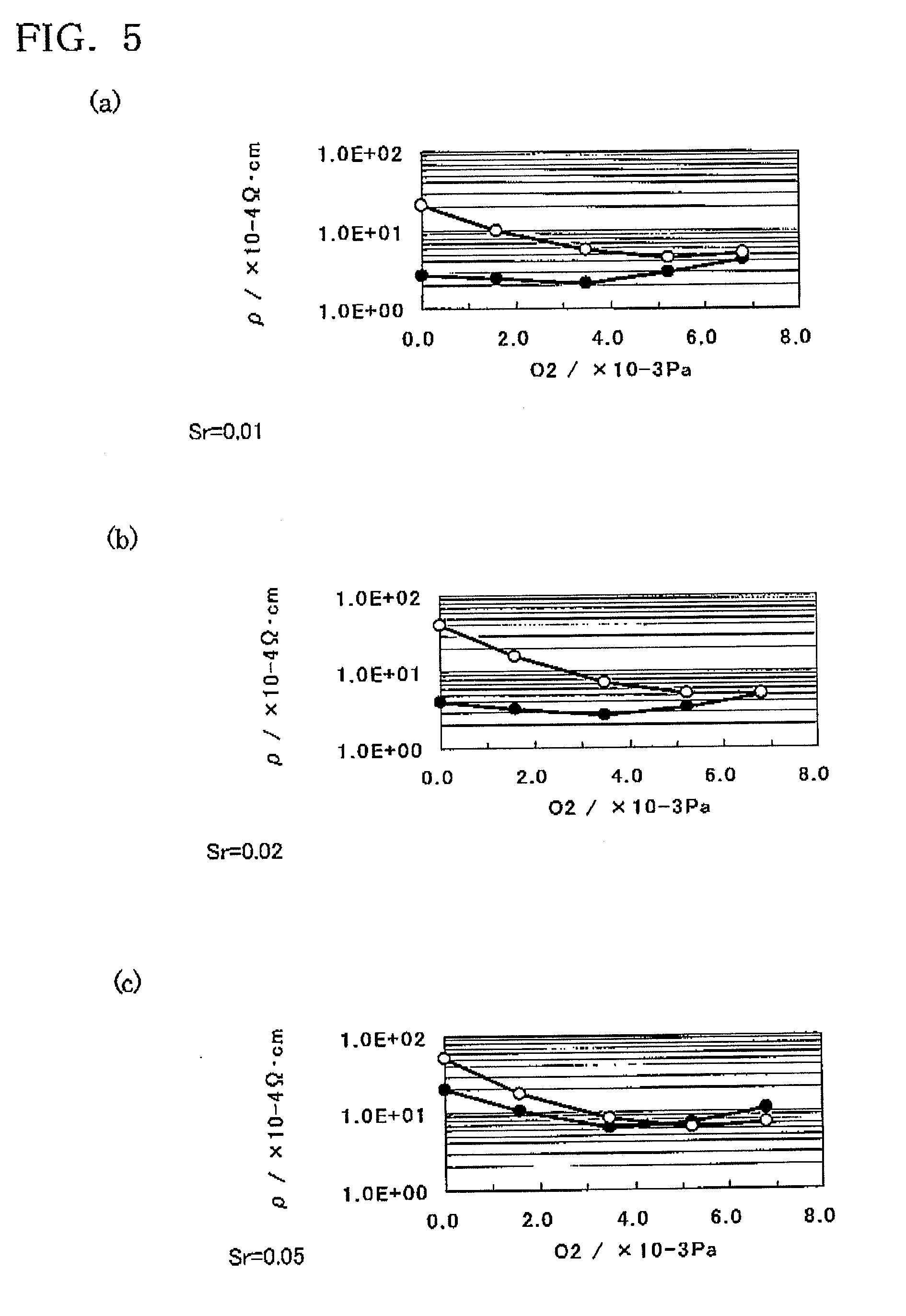
example 4

[0096]In2O3 powder (BET=5 m2 / g) and SnO2 powder (total: about 1.0 kg) were provided so that Sn was 0.25 mol on the basis of 1 mol of In. These powders were mixed by means of a ball mill. Subsequently, the mixture was mixed with an aqueous PVA solution serving as a binder, dried, and cold-pressed, to thereby prepare a compact. The compact was debindered in air at 600° C. for 10 hours with temperature elevation at 60 degrees (° C.) / h, and then fired in an oxygen atmosphere at 1,600° C. for eight hours, to thereby produce a sintered compact. In the firing process, specifically, the temperature was elevated from room temperature to 800° C. at 100 degrees (° C.) / h and from 800° C. to 1,600° C. at 400 degrees (° C.) / h, was kept at 1,600° C. for eight hours, and was lowered from 1,600° C. to room temperature at 100 degrees (° C.) / h. Thereafter, the sintered compact was processed, to thereby produce a target having a density of 7.14 g / cm3. The target was found to exhibit a bulk resistivity ...


PUM

PropertyMeasurementUnit
temperatureaaaaaaaaaa
transmittanceaaaaaaaaaa

Abstract

To provide a method for producing a method for producing a low-resistance and high-transmittance indium-oxide-based transparent conductive film readily obtained through crystallization, the method employing an amorphous film which can easily be patterned through etching with a weak acid.The method of the invention includes a step of confirming that a sputtering target which is provided and which contains indium oxide and an additive element can deposit an amorphous film at a predetermined film deposition temperature, and that the deposited amorphous film can be crystallized through annealing at a predetermined annealing temperature; a step of determining, as a film deposition oxygen partial pressure, an oxygen partial pressure at which a crystallized film obtained through annealing at the predetermined annealing temperature has the lowest resistivity, which oxygen partial pressure differs from an optimum oxygen partial pressure at which the amorphous film deposited at the predetermined film deposition temperature has the lowest resistivity; a step of depositing an amorphous film through sputtering the sputtering target at the film deposition oxygen partial pressure; and a step of crystallizing the amorphous film through annealing at the predetermined annealing temperature, to thereby form an indium-oxide-based transparent conductive film.

Description

TECHNICAL FIELD[0001]The present invention relates to a method for producing a low-resistance indium-oxide-based transparent conductive film readily obtained through crystallization, the method employing an amorphous film which can easily be patterned through etching with a weak acid.BACKGROUND ART[0002]Indium oxide-tin oxide (In2O3—SnO2 composite oxide, hereinafter abbreviated as “ITO”) film is a transparent conductive film which has high optical transparency with respect to visible light and high conductivity and which, therefore, finds a wide variety of applications, such as a liquid crystal display, a heat-generating film for defogging a glass panel, and an IR-reflecting film. However, difficulty is encountered in depositing such a transparent conductive film in an amorphous state.[0003]There has been proposed a technique in which an amorphous ITO thin film or a quasi-amorphous ITO thin film deposited of ITO microcrystals, whose crystallographic feature is determined through X-r...

Claims


Application Information

Patent Timeline
Patent Type & Authority Applications(United States)
IPC IPC(8): C23C14/08C23C14/34
CPCC23C14/086C23C14/5806C23C14/3414H01L31/1884
Inventor TAKAHASHI, SEIICHIROMIYASHITA, NORIHIKO
Owner MITSUI MINING & SMELTING CO LTD
Why Eureka
Try Eureka