Plating structure and method for manufacturing electric material

a technology of plating structure and manufacturing method, applied in the direction of incadescent envelope/vessel, transportation and packaging, coating, etc., can solve the problems of reducing the effect of preventing sulfurization, not necessarily achieving satisfactory effect, and reducing the reflectance of the layer, so as to avoid sulfurization and damage with time and temperature rise, high resistance, and low contact resistance

Inactive Publication Date: 2011-01-20
KYOWA ELECTRIC WIRE
View PDF13 Cites 23 Cited by
  • Summary
  • Abstract
  • Description
  • Claims
  • Application Information

AI Technical Summary

Benefits of technology

[0025]The present invention provides a plating structure whose surface is not sulfurized and damaged with time and rise in temperature. Further, the present invention provides a light-emitting element accommodating support including a reflecting surface having a plating structure highly resistant to heat, the light-emitting element accommodating support used for a light-emitting device that has a light-emitting element mounted thereon.
[0026]The present invention pr

Problems solved by technology

In a sulfur-containing environment, however, a silver-plated layer may be sulfurized with time and rise in temperature, and therefore the reflectance of the layer may decrease.
These remedies are effective to some extent, but do not necessarily achieve a satisfactory effect in the following respect.
This greatly reduces the effect of preventing sulfurization, and does not necessarily result in a sufficient effect of preventing the sulfurization of the reflecting surface, the sulf

Method used


Image

  • Plating structure and method for manufacturing electric material
  • Plating structure and method for manufacturing electric material
  • Plating structure and method for manufacturing electric material

Examples


experimental examples

Base Samples

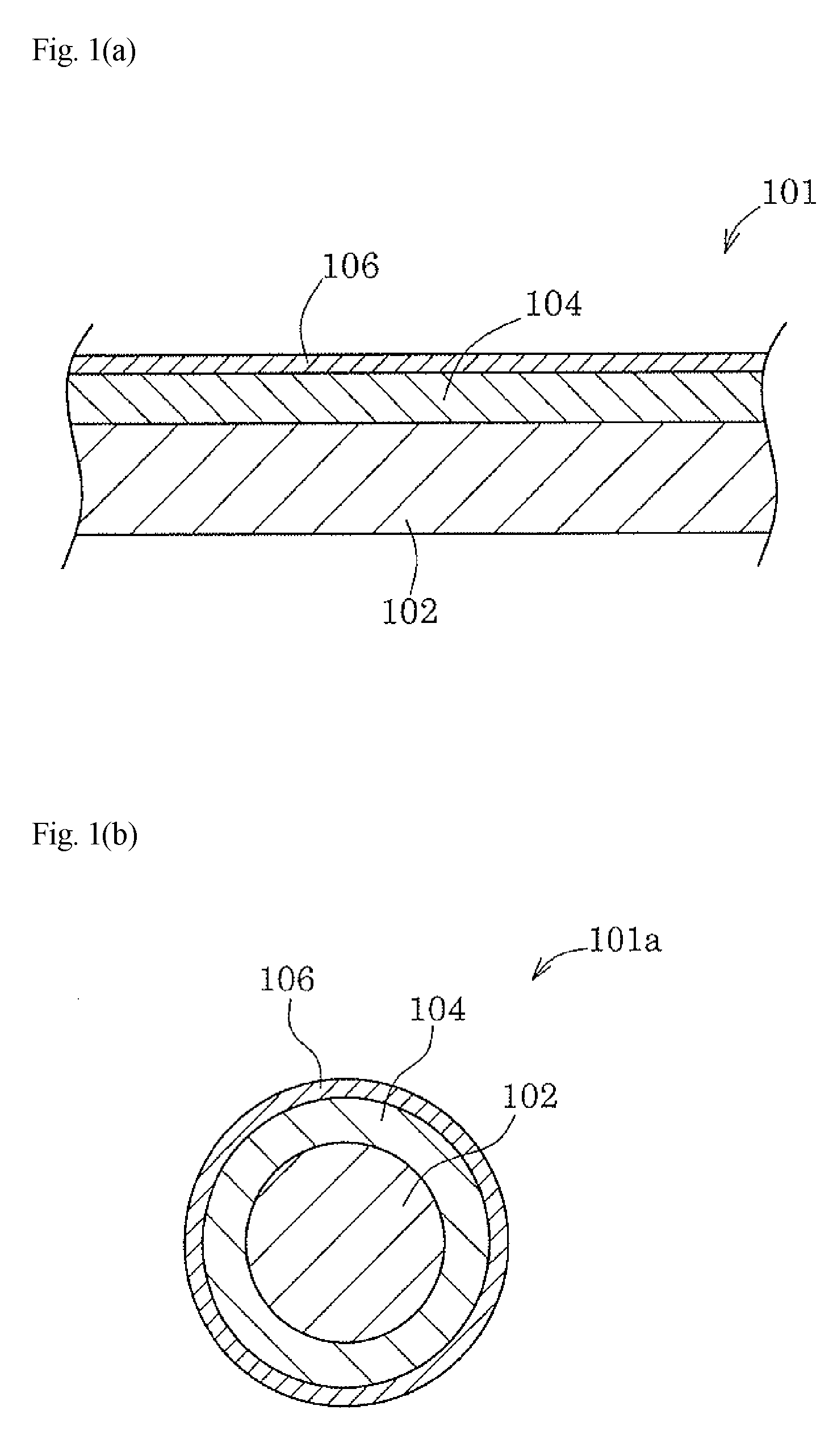
[0061]As an equivalent of the plating base 102 shown in FIG. 1(a) or FIG. 1(b), a 1-cm square piece of a lead frame copper alloy strip (product name “EFTEC3” manufactured by Furukawa Electric Co., Ltd.) was used. A base sample was obtained by underplating one side of the piece with copper to a thickness of 1 μm, and subsequently silver-plating the underplated side to a thickness of 2 μm. This base sample was tin-plated, heat-treated, and the like in accordance with the following experimental levels.

[0062]L-1: blank (the base sample).

[0063]L-2: a tin layer with a thickness of 0.01 μm was formed on the silver surface of the base sample by flash plating.

[0064]L-3: a tin layer with a thickness of 0.01 μm was formed on the silver surface of the base sample by flash plating, and subsequently the sample was heat-treated at 300° C. for 10 seconds.

[0065]L-4: a tin layer with a thickness of 0.02 μm was formed on the silver surface of the base sample by flash plating.

[0066]L-5: a t...

example 1

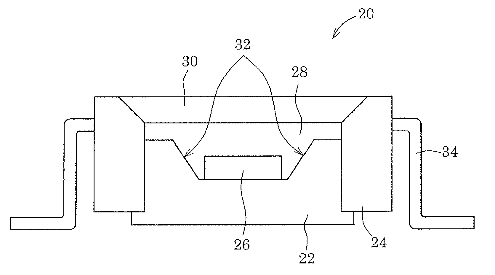
[0098]A frame in the shape of the substrate 203 shown in FIG. 2 was silver-plated and tin-plated. As the material of the frame that serves as the base, a lead frame copper alloy strip (“EFTEC3” manufactured by Furukawa Electric Co., Ltd.) was used, and the frame was formed by stamping the lead frame copper alloy strip. The frame was subjected to degreasing treatment, was subsequently acid rinsed with 5% sulfuric acid, and was underplated with copper in a bright copper sulfate bath (200 g / L copper sulfate, 50 g / L sulfuric acid, and a 2 mL / L commercial brightening agent). The film of the copper underplating had a thickness of 1.0 μm. Subsequently, the frame was bright silver-plated to a thickness of 2 μm in a bright silver cyanide bath (35 g / L silver cyanide, 90 g / L potassium cyanide, and 10 g / L potassium carbonate). Further, the frame was tin-plated to a thickness of 0.01 μm in an alkanolsulfonate bath (18 g / L tin(II), 100 g / L free acid, and 10 mL / L semi-brightening agent), and was s...

example 2

[0099]A stainless (SUS304) sheet with a thickness of 1 mm and 1 cm square was used as the base, was subjected to degreasing treatment, was subsequently acid rinsed with 5% sulfuric acid, and was underplated with copper in a bright copper sulfate bath (200 g / L copper sulfate, 50 g / L sulfuric acid, and a 2 mL / L commercial brightening agent). The film of the copper underplating had a thickness of 1.0 μm. Subsequently, the sheet was bright silver-plated to a thickness of 2 μm in a bright silver cyanide bath (35 g / L silver cyanide, 90 g / L potassium cyanide, and 10 g / L potassium carbonate). Further, the sheet was tin-plated to a thickness of 0.01 μm in an alkanolsulfonate bath (18 g / L tin(II), 100 g / L free acid, and 10 mL / L of semi-brightening agent), and was subsequently heat-treated at 500° C. for 10 seconds. Thus a bright sheet was obtained. A sulfurization test gave a similar result to that of L-3 of Table 1.


PUM

PropertyMeasurementUnit
Lengthaaaaaaaaaa
Diameteraaaaaaaaaa
Nanoscale particle sizeaaaaaaaaaa

Abstract

There is provided a plating structure obtained by heat-treating a silver-plated structure obtained by forming a tin-plated layer, an indium-plated layer, or a zinc-plated layer, having a thickness of 0.001 to 0.1 μm, on a surface of the silver-plated layer formed on a surface of a plating base. There is also provided a coating method for obtaining the plating structure which comprises the step of melting a particle deposit spottedly deposited at 2×10⁻⁶ to 8×10⁻⁶ g/cm2 such that the spot-deposited particles have gaps therebetween as viewed above and the particles each having an average diameter of 20 to 80 nm do not pile up in a direction perpendicular to the surface of the silver layer to obtain a film.

Description

BACKGROUND OF THE INVENTION[0001]1. Field of the Invention[0002]The present invention relates to a plating structure that reduces the deterioration of the surface properties thereof, and in particular, relates to a plating structure of an electric component material that requires sulfurization prevention, and also relates to a method for manufacturing an electric component material having the plating structure. Specifically, the present invention relates to a plating structure of a material suitable for use as: a metal lead frame; a lead wire using a metal strip; a lead wire provided on a non-conductive (e.g., ceramic) substrate; a lead pin; a reflecting plate; and the electric contact material of a terminal, a connector, or a switch, and also relates to a method for manufacturing the material. More specifically, the present invention relates to a plating structure of an electric component material highly resistant to sulfurization, and also relates to a method for manufacturing the...

Claims


Application Information

Patent Timeline
IPC IPC(8): H01J5/16B32B15/01B05D3/02
CPCB32B15/01Y10T428/12792C22F1/16C25D5/10C25D5/50C25D7/12H01L33/60H01L33/62H01L2224/48091H01L2224/48247C22F1/14Y10T428/12715Y10T428/12681H01L2924/00014C25D5/627C25D7/123C25D7/00
Inventor SUMIYA, YOSHINORISUGIE, KINYA
Owner KYOWA ELECTRIC WIRE
Why Eureka
Try Eureka