Optical devices featuring nonpolar textured semiconductor layers

Active Publication Date: 2011-02-03
TRUSTEES OF BOSTON UNIV
View PDF59 Cites 38 Cited by
  • Summary
  • Abstract
  • Description
  • Claims
  • Application Information

AI Technical Summary

Benefits of technology

[0014]The present invention provides a device for use as a light emitter. An emitter according to the invention is based on semiconductors prepared from textured nonpo

Problems solved by technology

The resulting facets may have an atomically smooth surface, with some l

Method used


Image

  • Optical devices featuring nonpolar textured semiconductor layers
  • Optical devices featuring nonpolar textured semiconductor layers
  • Optical devices featuring nonpolar textured semiconductor layers

Examples


example i

Growth of a Textured Nonpolar GaN Template by HVPE

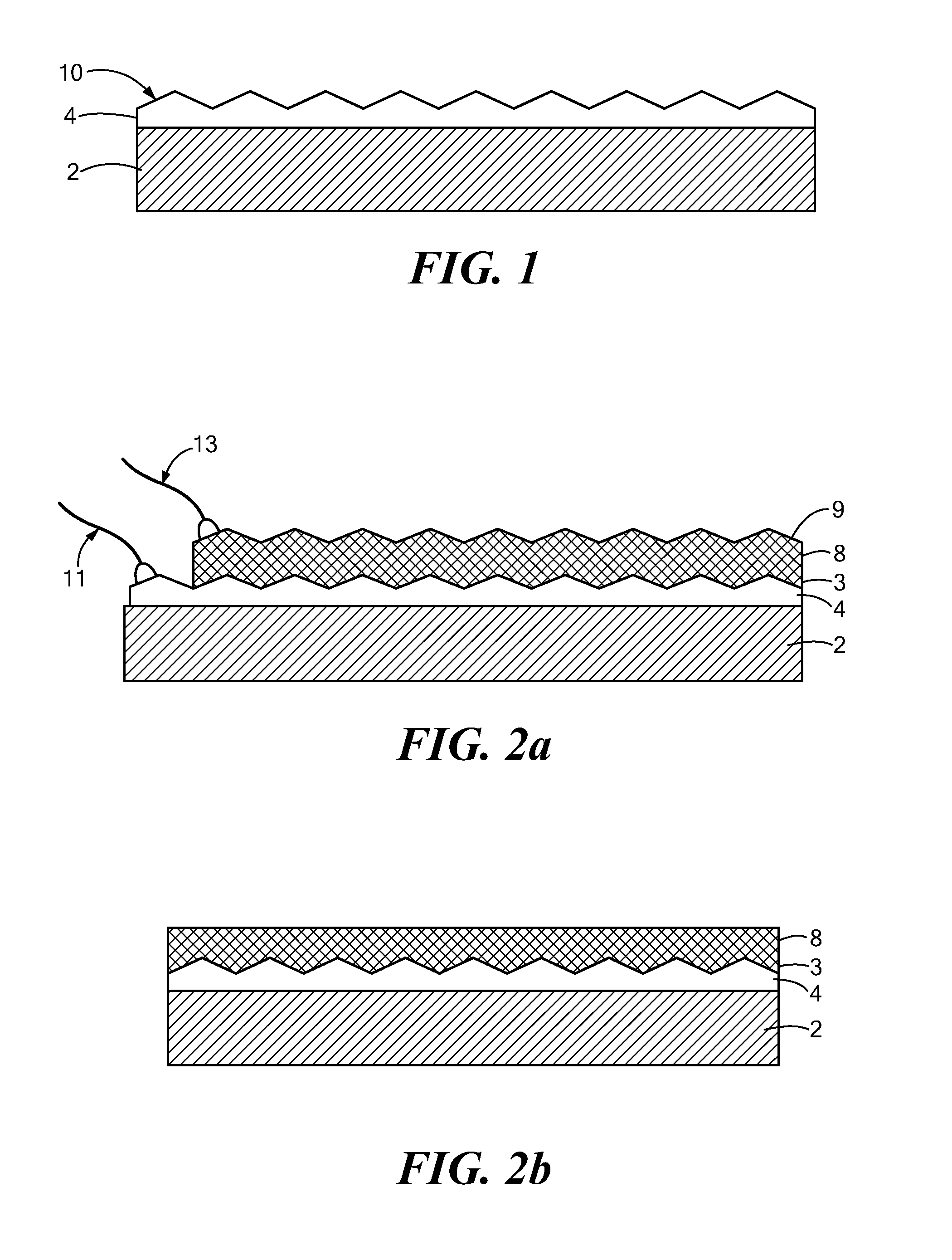
[0085]The textured non-polar A-plane GaN template was deposited on an R-plane sapphire substrate at 1000° C. by an HVPE method carried out in a vertical hydride vapor phase epitaxy (HVPE) reactor. The reactor consisted of concentric quartz tubes encased in a four zone furnace. Hydrogen chloride gas was carried into the centermost tube by nitrogen, where it reacted with liquid gallium in a boat to form GaCl. Ammonia was supplied through the outermost tube. A funnel was added at the point where the GaCl and NH3 meet to better shape the gas flows around the rotational sample stage.

[0086]A-GaN templates were grown directly onto (10-12) R-plane sapphire at a Zone 3 held at temperature of 1000° C. without the use of a GaN buffer layer. This is in contrast to the standard procedure of growing polar C—GaN templates which involves the growth of a low temperature GaN buffer layer before continuing with a high temperature growth phase. Gas flow...

example ii

Reflectance of Polar and Nonpolar GaN Templates

[0088]An atomically smooth C-plane GaN template about 50 μm thick was deposited using a three-step HVPE deposition process. In the first step, a sapphire substrate was subjected to nitridation by exposing the wafer to ammonia for 60 sec at 1000° C. In the second step, a buffer layer of 200 Å was deposited at 550° C., and in the third step the final epitaxial film was deposited at 1050° C.

[0089]The reflectance spectrum of the smooth C-plane template and that of the textured A-plane GaN template from Example I are compared in FIG. 7.

example iii

MQWs on a Textured Nonpolar GaN Template Emitting in the Deep UV

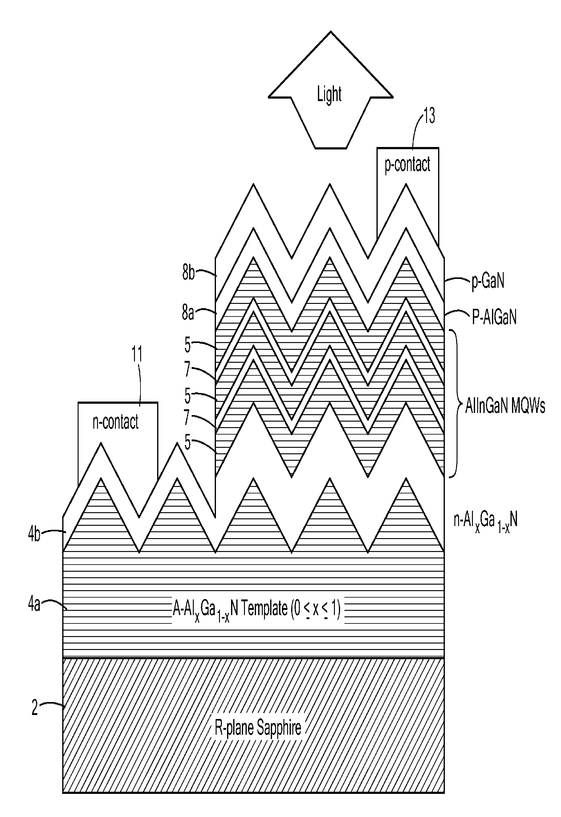
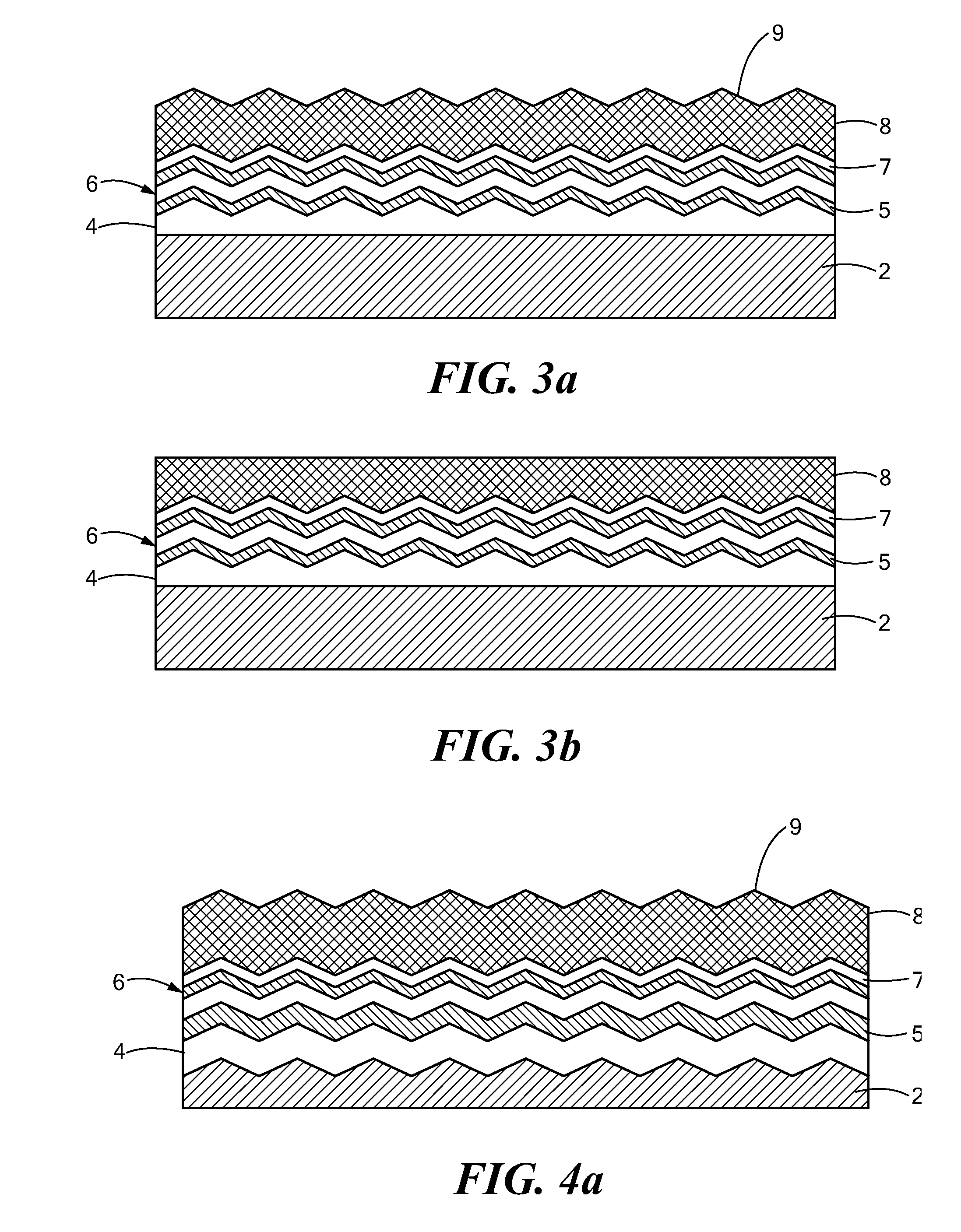
[0090]AlGaN / AlN MQWs were grown on a textured A-GaN template for emission in the deep UV. Similar procedures were used for the growth of AlGaN MQWs on the A-plane GaN template for near UV emission and InGaN MQWs for emission in the blue and green parts of the electromagnetic spectrum. In all cases the GaN templates were cleaned by standard degreasing steps before loading into the MBE system. Just before the growth was conducted, the surface was further cleaned by exposure to a gallium flux at a high temperature. The gallium reacted with impurities on the surface and then evaporated, leaving a pristine surface.

[0091]The wells were composed of AlGaN alloys with nominally 70% AlN mole-fraction, and barriers were of pure AlN. The well and barrier thicknesses were nominally 15 and 30 Å respectively, and 100 wells and barriers were employed.

[0092]The surface structure of the MQWs by electron microscopy is shown at various mag...


PUM


Abstract

A semiconductor emitter, or a precursor therefor, has a substrate and one or more textured semiconductor layers deposited onto the substrate in a nonpolar orientation. The textured layers enhance light extraction, and the use of nonpolar orientation greatly enhances internal quantum efficiency compared to conventional devices. Both the internal and external quantum efficiencies of emitters of the invention can be 70-80% or higher. The invention provides highly efficient light emitting diodes suitable for solid state lighting.

Description

CROSS REFERENCE TO RELATED APPLICATIONS[0001]This application claims the priority of U.S. Provisional Application No. 60 / 068,605 filed Mar. 7, 2008 and entitled, LOW-COST BLUE / UV LEDS WITH VERY HIGH PHOTON CONVERSION AND EXTRACTION EFFICIENCY FOR WHITE LIGHTING. This application further claims the priority of U.S. Provisional Application No. 60 / 732,034 filed Oct. 31, 2005 and entitled, OPTICAL DEVICES FEATURING TEXTURED SEMMICONDUCTOR LAYERS. This application is also a continuation-in-part of pending U.S. application Ser. No. 11 / 107,150 filed Apr. 15, 2005 and entitled OPTICAL DEVICES FEATURING TEXTURED SEMICONDUCTOR LAYERS, which claims the priority of U.S. Provisional Application No. 60 / 562,489 filed Apr. 15, 2004 and entitled, FORMATION OF TEXTURED III-NITRIDE TEMPLATES FOR THE FABRICATION OF EFFICIENT OPTICAL DEVICES, U.S. Provisional Application No. 60 / 615,047 filed Oct. 1, 2004 and entitled, FORMATION OF TEXTURED III-NITRIDE TEMPLATES FOR THE FABRICATION OF EFFICIENT OPTICAL D...

Claims


Application Information

Patent Timeline
IPC IPC(8): H01L33/04H01L21/20H01L33/16H01L33/20H01L33/24H01L33/32
CPCH01L21/02378H01L21/02389H01L21/02403H01L21/0242H01L21/02433H01L33/32H01L21/02609H01L33/16H01L33/20H01L33/24H01L21/0254
Inventor MOUSTAKAS, THEODORE D.MOLDAWER, ADAMBHATTACHARYYA, ANIRBANABELL, JOSHUA
Owner TRUSTEES OF BOSTON UNIV
Why Eureka
Try Eureka