System-in packages

a technology of system-in packages and packages, applied in the direction of basic electric elements, electrical apparatus contruction details, association of printed circuit non-printed electric components, etc., can solve the problems of significant challenges in manufacturability and structural reliability, and achieve the effect of easing the manufacturing of multi-layer chip integration and good uniformity of silicon thinning

Active Publication Date: 2011-02-03
QUALCOMM INC
View PDF8 Cites 351 Cited by
  • Summary
  • Abstract
  • Description
  • Claims
  • Application Information

AI Technical Summary

Benefits of technology

[0009]Furthermore, exemplary embodiments can provide for ease for manufacturing multi-layer chip integration.
[0010]Furthermore, exemplary embodiments can provide dummy substrates placed between chips to achieve good uniformity of silicon thinning.

Problems solved by technology

While WLP is a high throughput and low cost approach to IC chip packaging, it however invites significant challenges in manufacturability and structural reliability.

Method used


Image

  • System-in packages
  • System-in packages
  • System-in packages

Examples


first embodiment

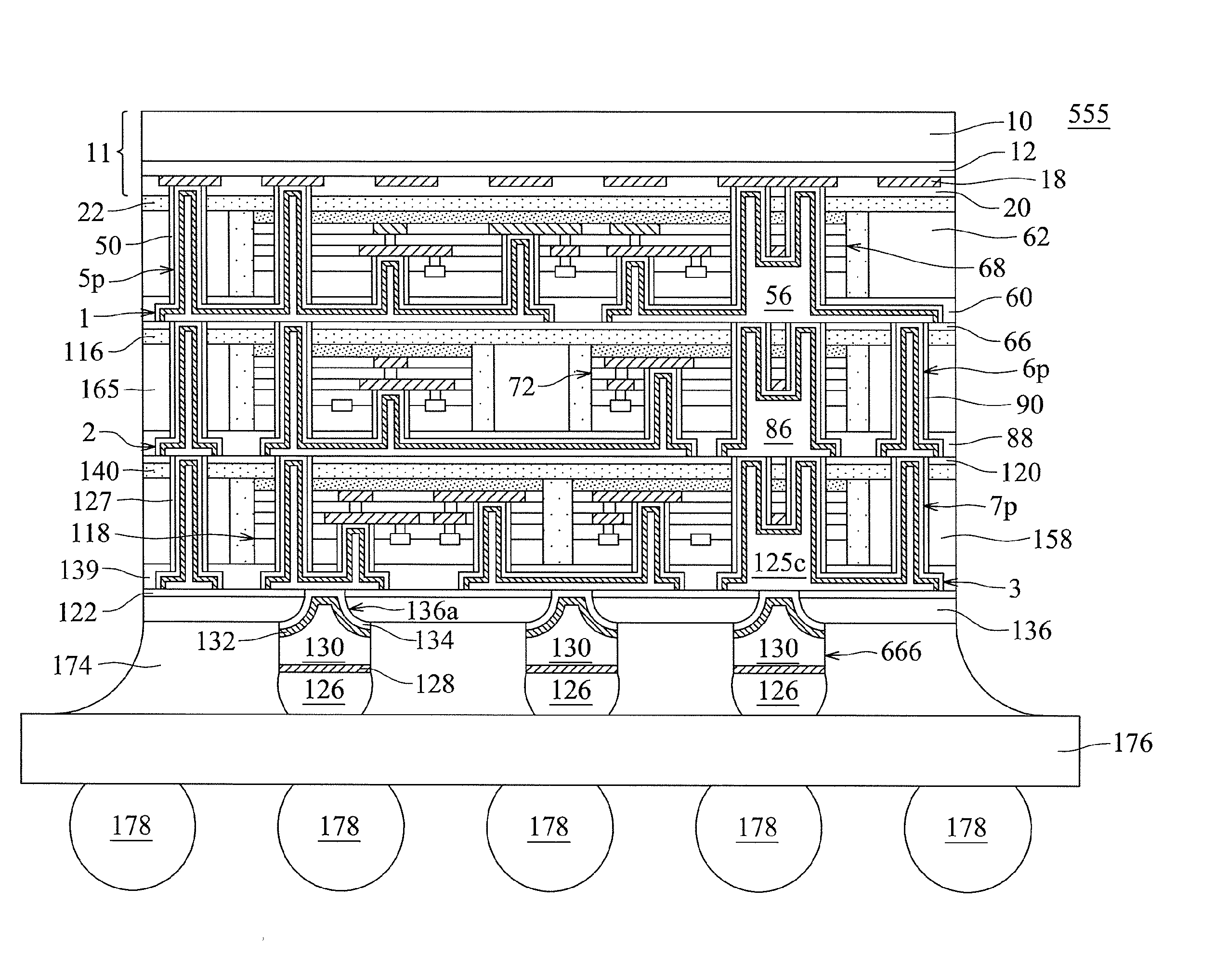
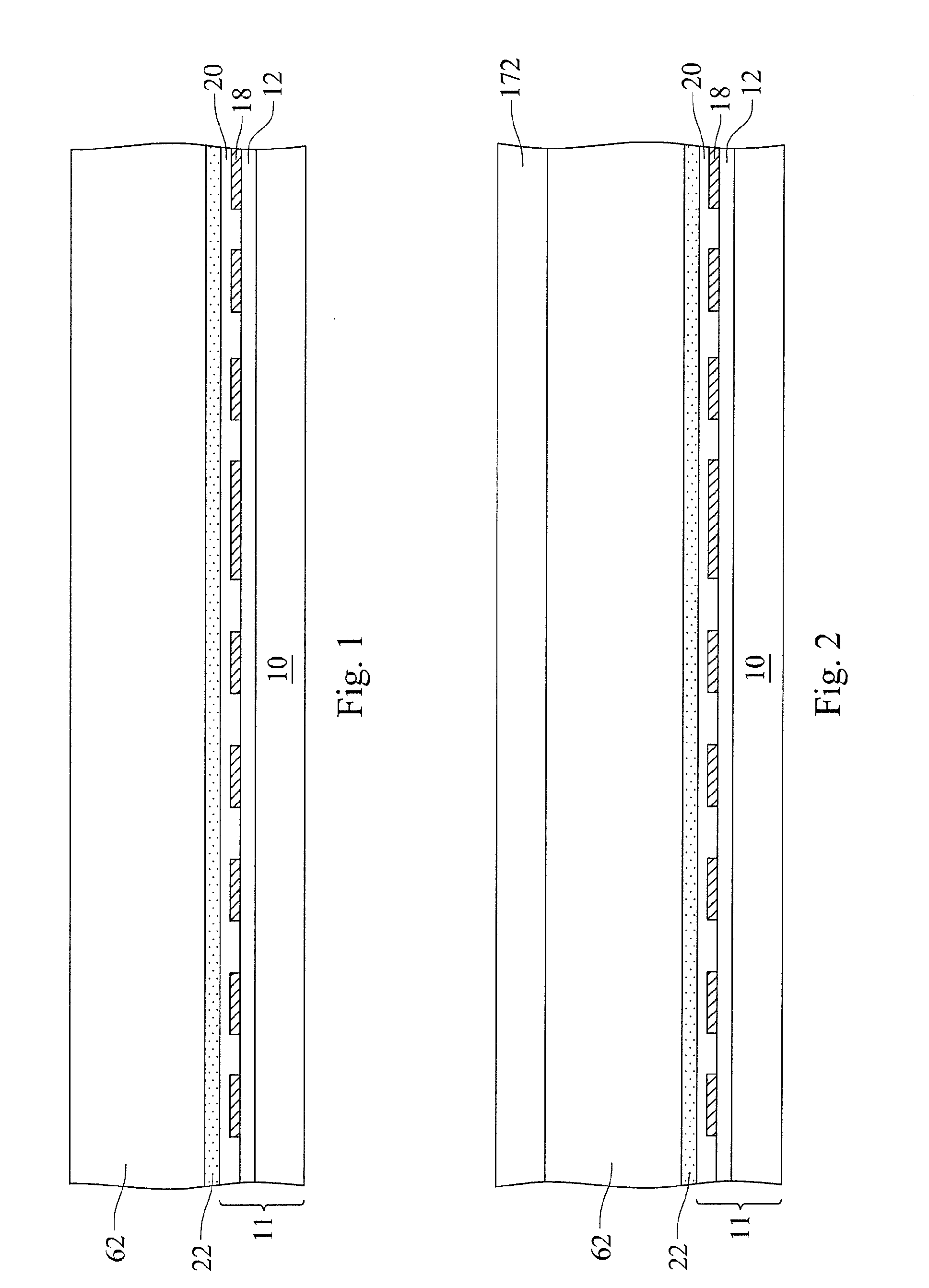
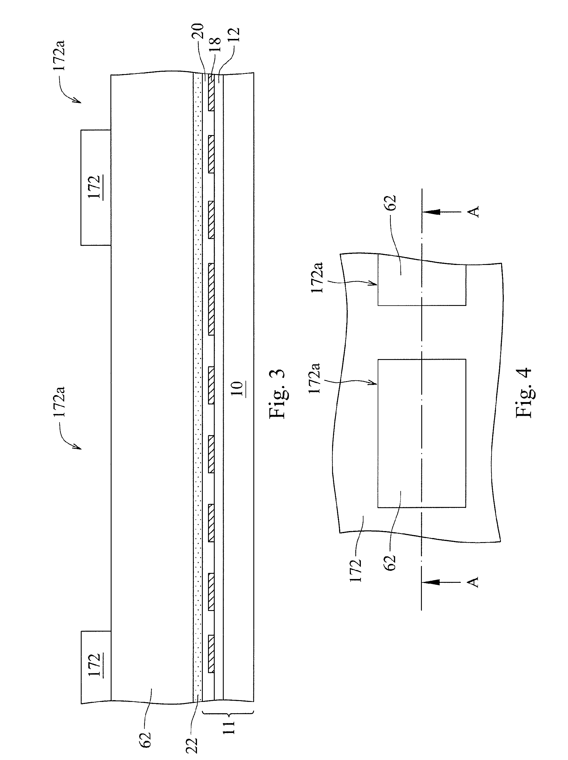
[0082]In a first embodiment, the carrier 11 can be a round wafer including the silicon substrate 10, multiple active devices, such as transistors, in and / or over the silicon substrate 10, the dielectric layer 12 on the silicon substrate 10, the patterned metal layer 18 on the dielectric layer 12, and the dielectric or insulating layer 20, such as a layer of silicon oxide (such as SiO2), silicon nitride (such as Si3N4), silicon oxynitride (such as SiON), silicon oxycarbide (such as SiOC), silicon carbon nitride (such as SiCN), or polymer (such as polyimide, benzocyclobutene, polybenzoxazole, or poly-phenylene oxide), on the patterned metal layer 18.

second embodiment

[0083]In a second embodiment, the carrier 11 can be a round wafer including the silicon substrate 10, multiple passive devices, such as resistors, inductors or capacitors, in and / or over the silicon substrate 10, the dielectric layer 12 on the silicon substrate 10, the patterned metal layer 18 on the dielectric layer 12, and the dielectric or insulating layer 20, such as a layer of silicon oxide (such as SiO2), silicon nitride (such as Si3N4), silicon carbon nitride (such as SiCN), silicon oxynitride (such as SiON), silicon oxycarbide (such as SiOC), or polymer (such as polyimide, benzocyclobutene, polybenzoxazole, or poly-phenylene oxide), on the patterned metal layer 18 and over the passive devices, but not including any active device, such as transistor, in and / or over the silicon substrate 10.

third embodiment

[0084]In a third embodiment, the carrier 11 can be a rectangular panel including the glass substrate 10, the dielectric layer 12 on the glass substrate 10, the conductive layer 18, such as indium-tin-oxide (ITO) layer, on the dielectric layer 12, and the dielectric or insulating layer 20 on the conductive layer 18.


PUM


Abstract

System-in packages, or multichip modules, are described which can include multi-layer chips and multi-layer dummy substrates over a carrier, multiple through vias blindly or completely through the multi-layer chips and completely through the multi-layer dummy substrates, multiple metal plugs in the through vias, and multiple metal interconnects, connected to the metal plugs, between the multi-layer chips. The multi-layer chips can be connected to each other or to an external circuit or structure, such as mother board, ball grid array (BGA) substrate, printed circuit board, metal substrate, glass substrate, or ceramic substrate, through the metal plugs and the metal interconnects.

Description

RELATED APPLICATION[0001]This application claims priority to U.S. provisional application No. 61 / 229,756, filed on Jul. 30, 2009, which is incorporated herein by reference in its entirety.BACKGROUND OF THE DISCLOSURE[0002]1. Field of the Disclosure[0003]The disclosure relates to system-in packages, and more particularly, to system-in packages that include through vias formed in stacked chips and in stacked dummy substrates and utilize metal plugs formed in the through vias for electrical interconnection between the stacked chips.[0004]2. Brief Description of the Related Art[0005]Semiconductor wafers are processed to produce IC (integrated circuit) chips having ever-increasing device density and shrinking feature geometries. Multiple conductive and insulating layers are required to enable the interconnection and isolation of the large number of semiconductor devices in different layers. Such large scale integration results in an increasing number of electrical connections between var...

Claims


Application Information

Patent Timeline
Patent Type & Authority Applications(United States)
IPC IPC(8): H05K7/02
CPCH01L2924/01072H01L2924/014H01L2224/45139H01L2924/01028H01L2924/10253H01L2924/1306H01L2924/13091H01L2924/1305H01L21/76898H01L23/3128H01L23/481H01L23/5389H01L23/60H01L24/16H01L24/45H01L24/48H01L24/94H01L24/96H01L25/0652H01L25/0655H01L25/0657H01L25/50H01L27/0251H01L2224/13099H01L2224/45124H01L2224/45144H01L2224/45147H01L2224/48091H01L2224/48227H01L2224/48465H01L2224/73257H01L2225/06513H01L2225/06541H01L2924/01011H01L2924/01013H01L2924/01014H01L2924/01015H01L2924/01022H01L2924/01029H01L2924/01032H01L2924/01042H01L2924/01047H01L2924/01049H01L2924/0105H01L2924/01073H01L2924/01074H01L2924/01075H01L2924/01077H01L2924/01078H01L2924/01079H01L2924/01082H01L2924/04941H01L2924/04953H01L2924/09701H01L2924/10329H01L2924/14H01L2924/15311H01L2924/19041H01L2924/19042H01L2924/19043H01L2924/30105H01L2224/16225H01L2224/32225H01L2224/73204H01L2224/73265H01L2224/9202H01L2924/01005H01L2924/01006H01L2924/01019H01L2924/01023H01L2924/01024H01L2924/01033H01L2924/00014H01L2924/00H01L2924/15747H01L2924/15787H01L2924/15788H01L2924/181H01L24/24H01L24/82H01L2224/24145H01L2224/24225H01L2924/12042H01L2924/3511H01L2224/05139H01L2224/05144H01L2224/05147H01L2224/05155H01L2224/05166H01L2224/05171H01L2224/05181H01L2224/05184H01L2224/05639H01L2224/05644H01L2224/05647H01L2224/05655H01L2224/05666H01L2224/05681H01L2924/00012H01L2924/00011H01L2924/013H01L2224/45015H01L2924/207H01L25/16H01L23/48H01L23/52H01L27/06
Inventor LIN, MOU-SHIUNGLEE, JIN-YUAN
Owner QUALCOMM INC
Why Eureka
Try Eureka