

Optical apparatus, optical detector, optical modulator, imaging apparatus, and camera
- Summary
- Abstract
- Description
- Claims
- Application Information
AI Technical Summary
Benefits of technology
Problems solved by technology
Method used
Image

Examples
first embodiment
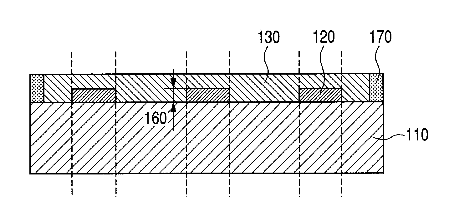
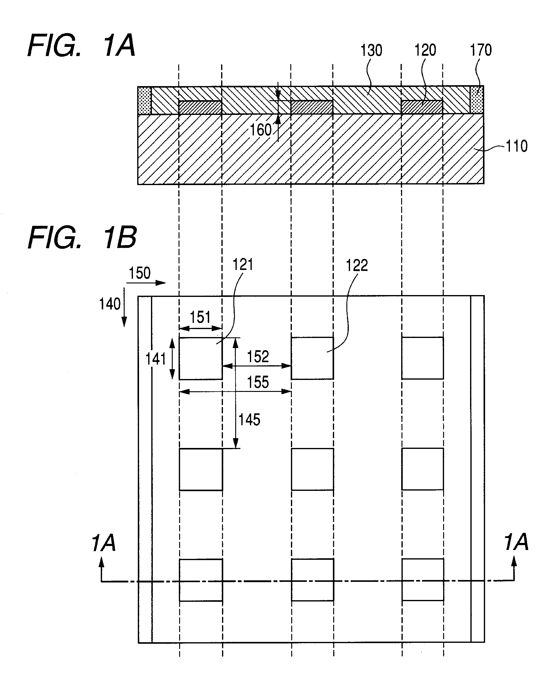
[0056]A structure of an optical filter according to a first embodiment of the present invention is described with reference to FIGS. 1A and 1B.
[0057]FIG. 1B is a top view of the optical filter according to this embodiment, and FIG. 1A is a cross sectional view taken along the dotted line in the top view of the optical filter.
[0058]As illustrated in FIG. 1A, on a surface of the dielectric substrate 110, multiple metal structures 120 are disposed, and a dielectric layer 130 is formed to cover the metal structures 120. The metal structures 120 are two-dimensionally disposed at regular intervals in a discrete manner in an in-plane direction of the dielectric substrate 110, and are configured as a metal structure group. Further, for description, two first metal structures constituting the first metal structure group are denoted by reference numerals 121 and 122.
[0059]Here, FIGS. 1A and 1B illustrates an example where the metal structures 120 are arranged at regular intervals.
[0060]In par...
second embodiment
[0087]In this embodiment, a structural example of an optical filter which has a liquid crystal layer as the protection layer is described.
[0088]As illustrated in FIG. 11A, metal structures 1102 are disposed on a dielectric substrate 1101, and a liquid crystal layer 1103 and a transparent electrode 1104 are further disposed on and above the dielectric substrate 1101. In addition, a transparent electrode 1105 is disposed also below the dielectric substrate 1101.
[0089]In this state, an electric field is applied to the liquid crystal layer 1103 so that the orientation of liquid crystal molecules in the liquid crystal layer is changed. Thus, the refractive index around each of the metal structures 1102 is changed, to thereby change the wavelength of the plasmon resonance to be induced in the metal structures 1102.
[0090]When the liquid crystal molecules are used, each of the liquid crystal molecules has a dipole moment. Therefore, the liquid crystal molecules may be oriented, to thereby g...
third embodiment
[0094]In this embodiment, a structural example of an optical filter which has a fluid layer as the protection layer is described.
[0095]As illustrated in FIG. 11B, metal structures 1107 are disposed on a dielectric substrate 1106, and a cover glass 1109 is disposed further thereabove, to thereby form a fluid path structure. Then, the fluid path structure is filled with a fluid 1108.
[0096]A type of the fluid 1108 flowing in the fluid path or temperature of the fluid 1108 may be changed so that a density thereof is changed, to thereby change the refractive index around each of the metal structures 1107. Thus, a wavelength of the plasmon resonance induced in the metal structures 1107 may be changed. For example, if the fluid is changed among water, ethanol, glycerol and the like, the refractive index around each of the metal structures 1107 may be changed largely, so that the wavelength of the plasmon resonance induced in the metal structures 1107 may be changed.
[0097]Therefore, accordi...
PUM
 Abstract
Description
Claims
Application Information