Substrate for thin-film photoelectric conversion device, thin-film photoelectric conversion device including the same, and method for producing substrate for thin-film photoelectric conversion device

a technology of photoelectric conversion device and substrate, which is applied in the direction of pv power plant, basic electric elements, final product manufacturing, etc., can solve the problems of difficult to remarkably change the shape of surface unevenness, affecting the formation of the photoelectric conversion device, and reducing the conversion efficiency of the thin-film photoelectric conversion device. , to achieve the effect of improving the ff and eff of the integrated-type thin-film photoelectric conversion device, improving the adhesion of th

Inactive Publication Date: 2011-03-31
KANEKA CORP
View PDF4 Cites 12 Cited by
  • Summary
  • Abstract
  • Description
  • Claims
  • Application Information

AI Technical Summary

Benefits of technology

[0047]In accordance with the present invention, the transparent insulating fine particles in the underlying layer are dispersed so as to cover one main surface of the transparent base member at a coverage factor in a range from 30% or more to 80% or less so that the fill factor (FF) and photoelectric conversion efficiency (Eff) of a thin-film photoelectric conversion device to be formed on the underlying layer can be improved. That is, by setting the coverage factor of fine particles to less than 80%, it is possible to suppress the particles from being partially stacked in severalfold, and by setting the coverage factor thereof to 30% or more, it is possible to form a zinc oxide transparent electrode layer with surface unevenness that is effectively used for exerting a light confinement characteristic, and also to improve the adhesion of the electrode layer. Moreover, when the insulating particles are suppressed from being partially stacked in severalfold, it is possible to suppress an insufficient laser scribing process upon manufacturing an integrated-type thin-film photoelectric conversion device, and consequently to improve the FF and Eff of the integrated-type thin-film photoelectric conversion device.
[0048]Furthermore, by setting the average particle size of the transparent insulating fine particles in the underlying layer in a range from 50 nm to 200 nm, it is possible to easily set the coverage factor of the particles in a range from 30% to 80%. In the case where the zinc oxide transparent electrode layer is deposited by using a low-pressure CVD method, a ZnO layer having preferable surface unevenness can be easily formed on the underlying layer containing fine particles, at a high film-forming rate.
[0049]In contrast, by making the coverage factor of particles of the antireflection layer greater than that of the underlying layer, preferably, by setting the coverage factor of particles of the antireflection layer to 80% or more, the reflectance of light to be made incident on the antireflection layer can be reduced so that the Jsc is increased and the characteristics of the thin-film photoelectric conversion device can be further improved.

Problems solved by technology

In the amorphous silicon thin-film photoelectric conversion device, the initial photoelectric conversion efficiency is lower than that of a photoelectric conversion device that utilizes monocrystalline or polycrystalline silicon, and a problem exists in that the conversion efficiency is lowered due to a photodegradation phenomenon when irradiated with light for a long period of time.
In the thin-film photoelectric conversion device as described above, it becomes possible to make the photoelectric conversion layer thinner in comparison with a conventional photoelectric conversion device in which a bulk monocrystalline or polycrystalline silicon substrate is utilized; however, a problem is raised in that light absorption is limited by the film thickness.
However, although it is preferable to increase the surface unevenness so as to further enhance the light confinement effect, only the use of the SnO2 film solely makes it difficult to remarkably change the shapes of the surface unevenness, while light-transmitting property and conductivity required for the photoelectric conversion device are being properly maintained.
Moreover, in the case where an SnO2 film is formed on a glass plate as the transparent electrode layer having surface unevenness that is effective for the light confinement by using a normal-pressure thermal chemical vapor deposition method (normal-pressure thermal CVD method), since the thermal CVD method uses a high-temperature process in a range of about 550 to 650° C., a problem is raised in that the formation cost of the transparent electrode layer becomes high.
Moreover, in the case where the film-forming temperature is high, another problem is that it becomes difficult to use inexpensive base members, such as normal glass plates and plastic films.
Furthermore, when a reinforced glass plate is subjected to a high temperature process, its reinforcing effect is lost.
Consequently, in the case where a base member of a glass plate is applied to a solar cell with a large area during a high-temperature process, the thickness of the glass plate needs to be increased so as to maintain its strength, causing a problem in that the glass plate becomes heavier.
Moreover, since the SnO2 film is poor in plasma resistant property, the SnO2 film may be reduced under a high plasma concentration containing hydrogen in a deposition environment of the photoelectric conversion layer.
Since the SnO2 film is blackened when reduced, incident light is absorbed by the blackened electrode layer, with the result that the quantity of transmitted light into the photoelectric conversion layer is reduced to cause a reduction in the photoelectric conversion efficiency.

Method used


Image

  • Substrate for thin-film photoelectric conversion device, thin-film photoelectric conversion device including the same, and method for producing substrate for thin-film photoelectric conversion device
  • Substrate for thin-film photoelectric conversion device, thin-film photoelectric conversion device including the same, and method for producing substrate for thin-film photoelectric conversion device
  • Substrate for thin-film photoelectric conversion device, thin-film photoelectric conversion device including the same, and method for producing substrate for thin-film photoelectric conversion device

Examples


experimental example 1

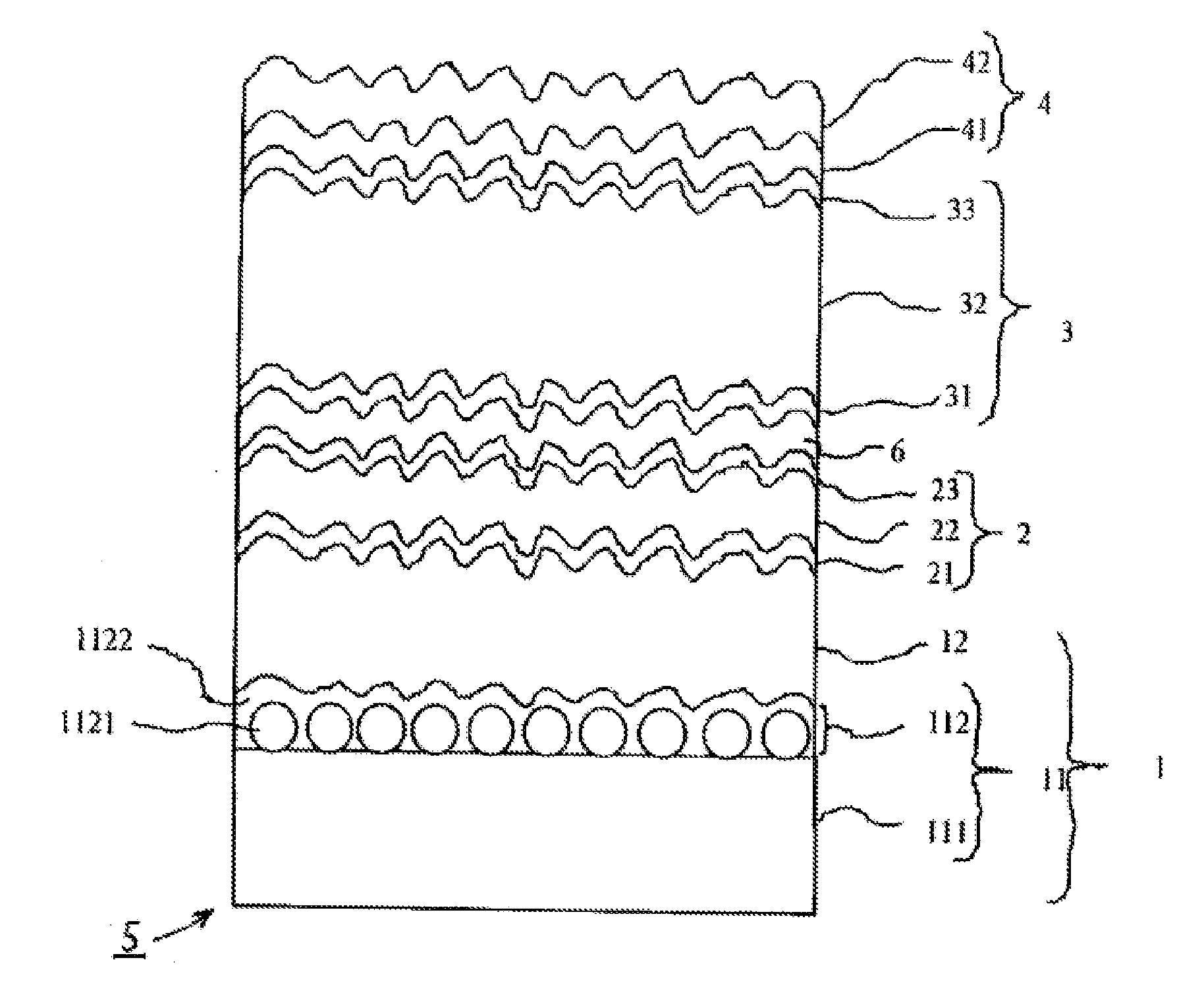
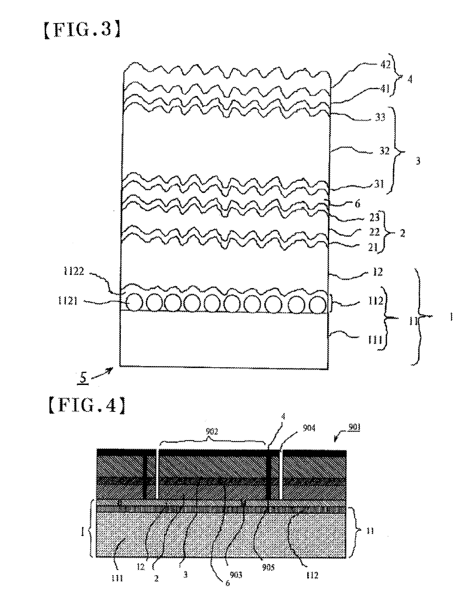
[0116]A substrate 1 for a thin-film photoelectric conversion device, as shown in FIG. 3, was manufactured as Experimental Example 1 of the present invention. First, a transparent underlying layer 112 containing SiO2 fine particles 1121 and a binder 1122 was formed on a glass plate 111 having a thickness of 4 mm and an area of 910 mm×455 mm so as to obtain a transparent insulating base member 11. A coating solution to be used upon forming the transparent underlying layer 112 was prepared by processes in which tetraethoxy silane was added to a mixed solution of a dispersion solution of spherical silica having an average particle size of 100 nm, water and ethylcellosolve, and thereafter hydrochloric acid was added so that tetraethoxy silane was hydrolyzed, and diacetone alcohol and propylene glycol were further added as diluting solutions. The mass concentration of spherical silica relative to the coating solution as a whole was 6%. After the coating solution had been applied onto the ...

experimental example 2

[0121]In Experimental Example 2 of the present invention, a substrate 1 for a thin-film photoelectric conversion device similar to that of Experimental Example 1 was manufactured. That is, the substrate of Experimental Example 2 was different from that of Experimental Example 1 only in that the mass concentration of spherical silica relative to the coating solution as a whole was changed from 6% to 2%.

[0122]FIG. 7, which is similar to FIG. 5, shows an AFM image of the upper surface of a transparent insulating base member 11 obtained in Experimental Example 2. In comparison with that of FIG. 5 of Experimental Example 1, in FIG. 7 of Experimental Example 2, gaps among the silica fine particles were clearly widened, and in this case, the coverage factor of particles was 49.3%.

[0123]As a reference, FIG. 8 shows an SEM image of the upper surface of the transparent insulating base member 11 obtained in Experimental Example 2. In the SEM image of FIG. 8 as well, the same particle distribut...

reference example 1

[0125]In Reference Example 1, a substrate 1 for a thin-film photoelectric conversion device similar to that of Experimental Example 1 was manufactured. That is, the substrate of Reference Example 1 was different from that of Experimental Example 1 in that the average particle size of spherical silica was changed from 100 nm to 50 nm, and in that the mass concentration of spherical silica relative to the coating solution as a whole was changed from 6% to 4%.

[0126]The surface of the transparent insulating base member 11 obtained in Reference Example 1 was measured by AFM to find that the coverage factor of the particles was 98.9%.

[0127]On the transparent insulating base member 11 obtained in Reference Example 1, a transparent electrode layer 12 made of ZnO was deposited in the same method as that of Experimental Example 1. As a result, in the ZnO film transparent electrode layer 12 obtained in Reference Example 1, the thickness, obtained from interference of reflection spectra, was 1....


PUM


Abstract

Provided is a substrate for a thin-film photoelectric conversion device which makes it possible to produce the device having improved characteristics at low cost and high productivity. The substrate includes a transparent base member, with a transparent underlying layer and a transparent electrode layer successively stacked on one main surface of the transparent base member. The underlying layer includes transparent insulating fine particles and transparent binder, and the particles are dispersed to cover the one main surface with a coverage factor of particles—ranging from 30% or more to less than 80%. An antireflection layer is provided on the other main surface of the transparent base. The antireflection layer includes transparent insulating fine particles and transparent binder, and the particles are dispersed to cover the other main surface with a coverage factor greater than the underlying layer. The transparent electrode layer contains zinc oxide deposited by low-pressure CVD method.

Description

TECHNICAL FIELD[0001]The present invention relates to an improved substrate for a thin-film photoelectric conversion device, and the thin-film photoelectric conversion device including such an improved substrate, and also relates to a method for producing the substrate for a thin-film photoelectric conversion device.BACKGROUND ART[0002]Photoelectric conversion devices have been used in various fields such as light-receiving sensors and solar cells. Among these, the solar cells have drawn public attention as one of the energy sources that are friendly to the earth. Moreover, together with increased concerns about environmental-related issues in recent years and accelerating policies for introducing solar cells in various countries, solar cells have been widely used rapidly.[0003]In recent years, in order to achieve both of reduced costs and high efficiency of the photoelectric conversion devices, public attention has been drawn to a thin-film photoelectric conversion device which req...

Claims


Application Information

Patent Timeline
Patent Type & Authority Applications(United States)
IPC IPC(8): H01L31/052H01L31/18H01L31/0232
CPCH01L31/02168H01L31/03921H01L31/046Y02E10/548H01L31/076H01L31/1804H01L31/0463Y02E10/547Y02P70/50
Inventor KIKUCHI, TAKASHISASAKI, TOSHIAKI
Owner KANEKA CORP
Why Eureka
Try Eureka