
Film forming method of silicon oxide film, silicon oxide film, semiconductor device, and manufacturing method of semiconductor device

a technology of silicon oxide film and film forming method, which is applied in the direction of silicon oxide, silicon compounds, coatings, etc., can solve the problems of deterioration of the characteristics of the formed transistor in the latter process, inferior film quality, and low quality of the formed film. achieve excellent quality

Inactive Publication Date: 2011-03-31
TOKYO ELECTRON LTD
View PDF11 Cites 15 Cited by
  • Summary
  • Abstract
  • Description
  • Claims
  • Application Information

AI Technical Summary

Benefits of technology

[0047]According to the film forming method of the silicon oxide film, the silicon oxide film, the semiconductor device, and the production method of the semiconductor device in the present invention, a thin film composed of a silicon oxide having an excellent quality can be formed by a low-temperature CVD method even in a semiconductor device having a metal wiring (a part formed of metal such as a metal gate may be contained).

Problems solved by technology

In general, it is known that a CVD oxide film and a CVD nitride film formed by a film forming method of a low-temperature CVD method where the assist of active oxygen such as plasma and ozone is necessary, is inferior in film quality (electric characteristics here) to a film formed by a HTO-CVD method such as a thermal CVD method, in a process after a gate forming step (BEOL) in a semiconductor element such as an LSI and a CMOS image sensor in which a metal (metal material) having a low melting point (450° C. or less) is used as a gate wiring material of a transistor.
In addition, it is known that according to a plasma CVD film formed by a plasma CVD method, the characteristics of a formed transistor deteriorates in a latter process (BEOL) due to damage caused by plasma processing.

Method used


Image

  • Film forming method of silicon oxide film, silicon oxide film, semiconductor device, and manufacturing method of semiconductor device
  • Film forming method of silicon oxide film, silicon oxide film, semiconductor device, and manufacturing method of semiconductor device
  • Film forming method of silicon oxide film, silicon oxide film, semiconductor device, and manufacturing method of semiconductor device

Examples


first embodiment

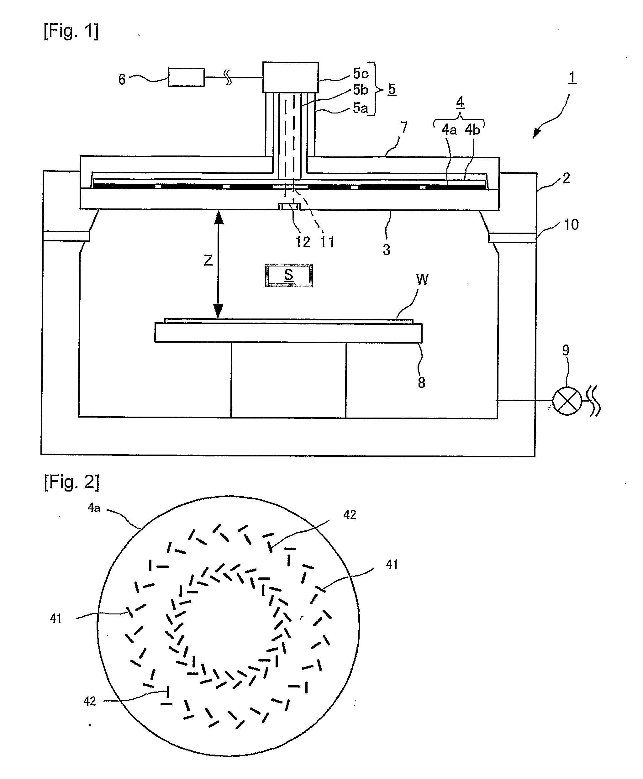
[0079]FIG. 1 is a sectional view showing a plasma processing apparatus according to a first embodiment of the present invention. The plasma processing apparatus is a plasma processing apparatus in which a silicon oxide film is formed on a target substrate with plasma generated by Radial Line Slot Antenna (RLSA). FIG. 2 is a plan view showing one example of a slot plate serving as a part of the plasma processing apparatus.

[0080]A plasma processing apparatus 1 includes a chamber 2, a top plate (dielectric window) 3, an antenna 4, a waveguide 5, a microwave source 6, a cooling jacket 7, a substrate holder 8, and a vacuum pump 9. Gas can be supplied from a gas supply source (not shown) into the chamber 2 through a wall gas passage 10 or a center gas passage 11.

[0081]The antenna 4 is provided on the top plate 3, and the cooling jacket 7 having a passage for passing a temperature adjustment medium is provided on the antenna 4. The antenna 4 includes a slot plate 4a and a wave length short...

working example

[0107]The characteristics of the silicon oxide film formed by the method according to the first embodiment are evaluated as follows.

[0108]FIG. 8 shows current characteristics (J) in a film thickness region of 7 nm±1 nm in terms of EOT (Equivalent Oxide Thickness) while the intensity of the applied electric field is changed. The density of a current flowing in the film when an electric field of 7 MV / cm is applied is measured. Here the target substrate W is a P-type semiconductor.

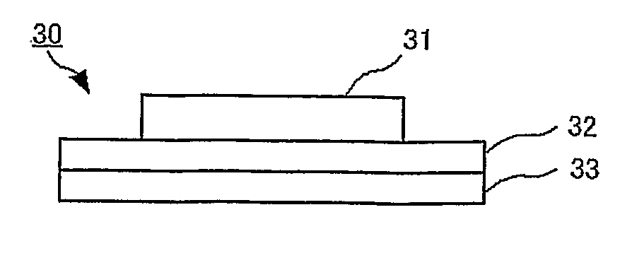
[0109]The reference character R_TEOS in the drawing designates the silicon oxide film according to the present invention, and a WVG film is shown for comparison. As the element for measuring the electric characteristics, a MOSCAP element used when the electric characteristics are measured in general is formed, and the current-voltage (I-V) characteristics are measured. A MOSCAP element 30 is shown in FIG. 9.

[0110]The MOSCAP element 30 is composed of a diffusion layer 31 of an N-type semiconductor, a gate oxid...

second embodiment

[0122]FIG. 13 is a sectional view showing a semiconductor device according to a second embodiment of the present invention. A description will be made of a production example of an MOS type semiconductor device in which the film forming method of the silicon oxide film according to the first embodiment is used, with reference to the drawing. The film is formed with the RLSA microwave plasma in the plasma processing apparatus shown in FIG. 1. In addition, a Si substrate 50 is a P-type semiconductor substrate.

[0123]First, the Si substrate 50 in which an element isolation region 51 is formed is prepared (FIG. 13A). At this time, a transistor formation part 52 on a main surface of the Si substrate 50 is formed of Si, SiON, SiO and the like.

[0124]Then, as described above for the film forming method of the silicon oxide film in the first embodiment, a gate insulating film 53 composed of the silicon oxide film is formed with TEOS (tetraethoxysilane) by the plasma CVD method (FIG. 13B).

[012...


PUM

PropertyMeasurementUnit
Temperatureaaaaaaaaaa

Abstract

A silicon compound gas, an oxidizing gas, and a rare gas are supplied into a chamber (2) of a plasma processing apparatus (1). A microwave is supplied into the chamber (2), and a silicon oxide film is formed on a target substrate with plasma generated by the microwave. A partial pressure ratio of the rare gas is 10% or more of a total gas pressure of the silicon compound gas, the oxidizing gas, and the rare gas, and an effective flow ratio of the silicon compound gas and the oxidizing gas (oxidizing gas / silicon compound gas) is not less than 3 but not more than 11.

Description

TECHNICAL FIELD[0001]The present invention relates to a film forming method of a silicon oxide film, a silicon oxide film, a semiconductor device, and a manufacturing method of a semiconductor device.BACKGROUND ART[0002]As a method for forming an insulating film such as a silicon oxide film and a nitride film in a transistor element isolation region or an interlayer insulating film between wirings in a semiconductor manufacturing process, a thermal CVD method is usually used to form a high-quality insulating film in the case where a high-temperature heat treatment at 750° C. or more is allowed in the process. In addition, in the case where a high-temperature heat treatment at 450° C. to 750° C. is allowed in the process, a thermal CVD film is formed at a temperature of 420° C. to 500° C. by CVD method at a normal-pressure, and then the quality of the insulating film is improved by a heat treatment at about 750° C. in general.[0003]Recently, it is highly required to operate an elemen...

Claims


Application Information

Patent Timeline
IPC IPC(8): H01L21/31C01B33/113H01L23/48
CPCC23C16/402C23C16/511H01L21/02164H01L21/76224H01L21/28273H01L21/31612H01L21/02274H01L29/40114H01L21/02216H01L21/324H01L21/76829
Inventor UEDA, HIROKAZUTANAKA, YOSHINOBUOHSAWA, YUSUKENOZAWA, TOSHIHISAMATSUOKA, TAKAAKI
Owner TOKYO ELECTRON LTD
Learn More