

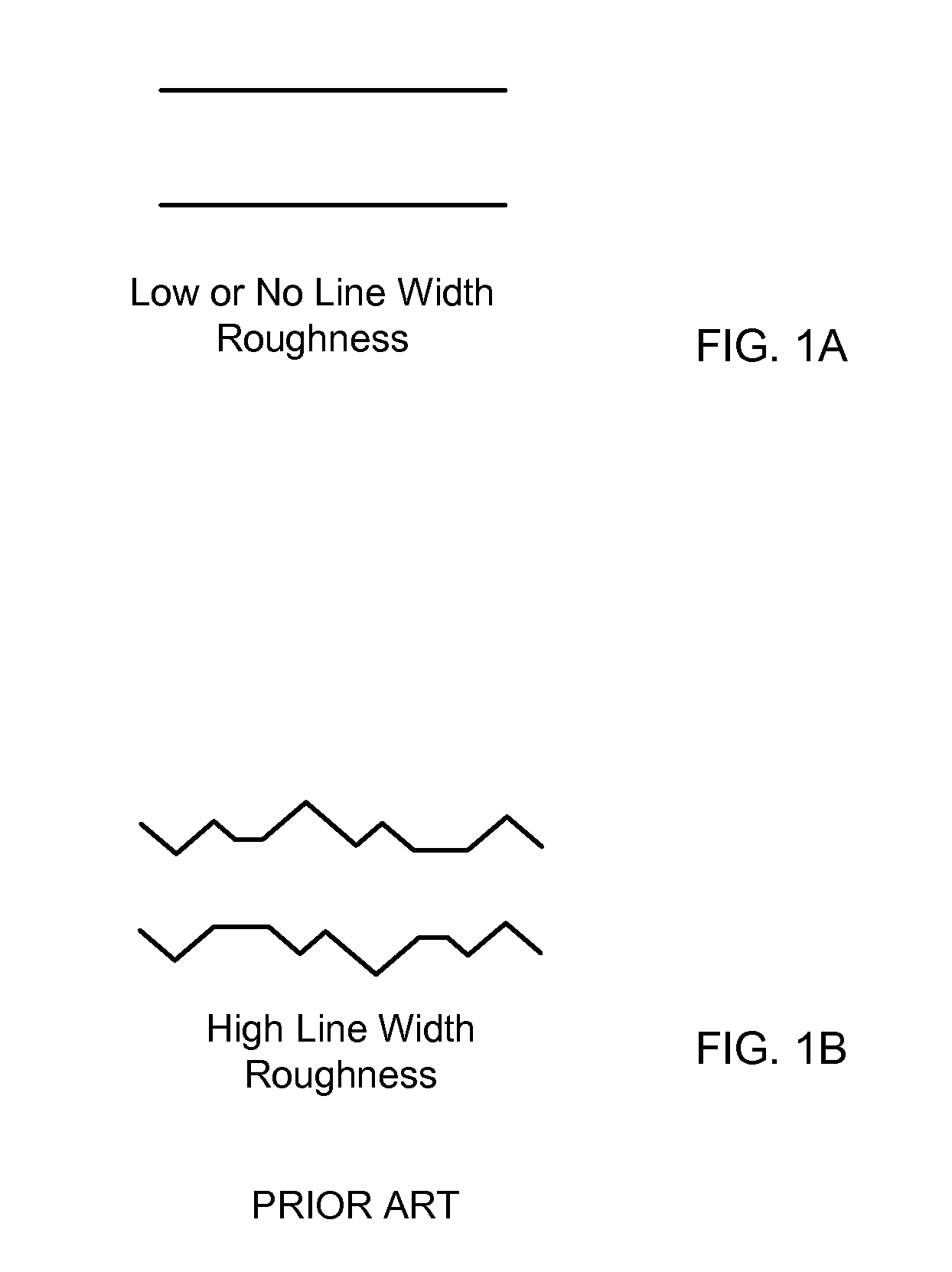
Line width roughness improvement with noble gas plasma
a plasma and noble gas technology, applied in the field of etching, can solve the problems of linear features patterned by photolithography, the roughness of the edges of lines, and the formation of “feet” at the base of the photoresist layer, and achieve the effect of reducing the roughness of the line width
- Summary
- Abstract
- Description
- Claims
- Application Information
AI Technical Summary
Benefits of technology
Problems solved by technology
Method used
Image

Examples
Embodiment Construction
[0021]The present invention will now be described in detail with reference to a few preferred embodiments thereof as illustrated in the accompanying drawings. In the following description, numerous specific details are set forth in order to provide a thorough understanding of the present invention. It will be apparent, however, to one skilled in the art, that the present invention may be practiced without some or all of these specific details. In other instances, well known process steps and / or structures have not been described in detail in order to not unnecessarily obscure the present invention.
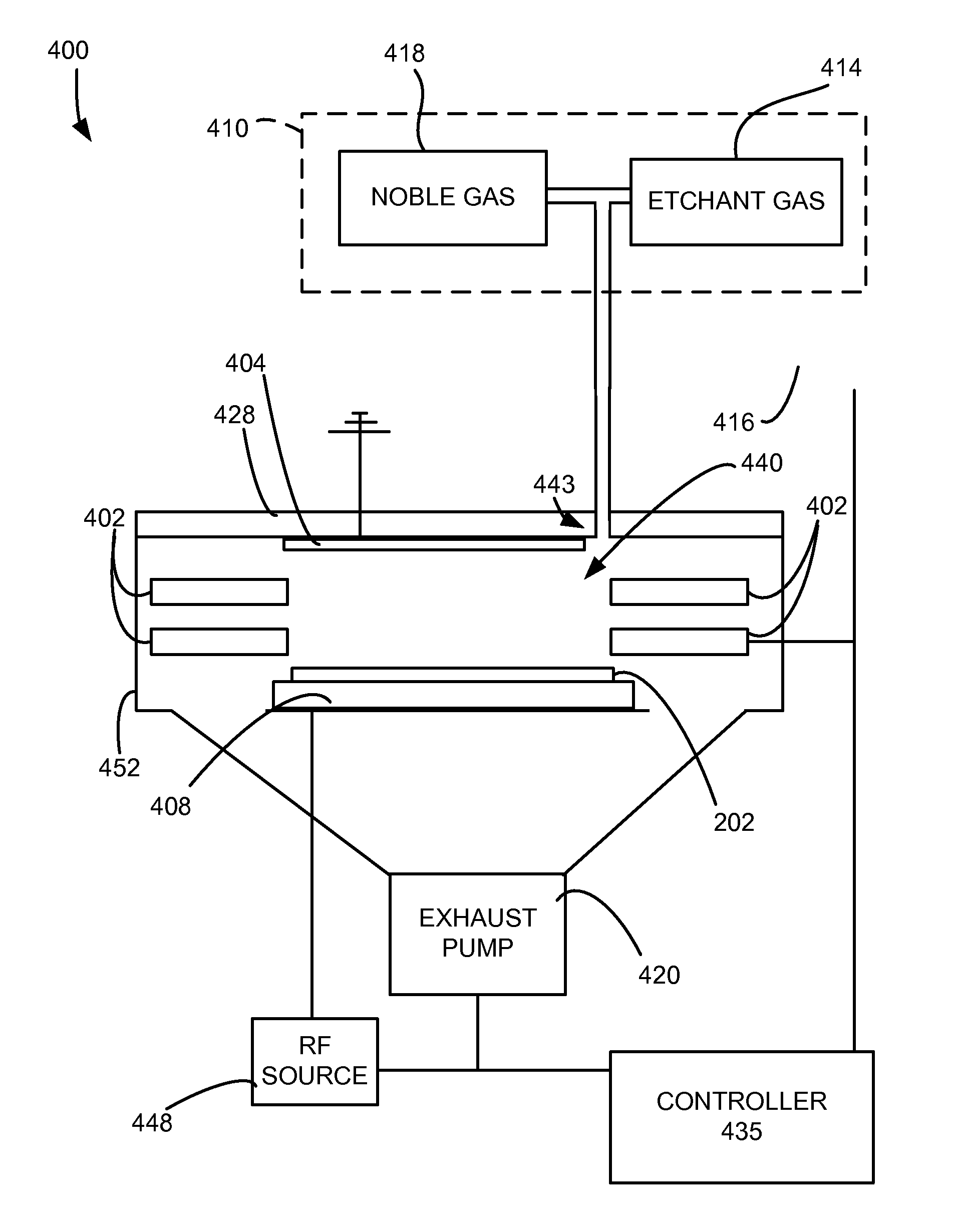
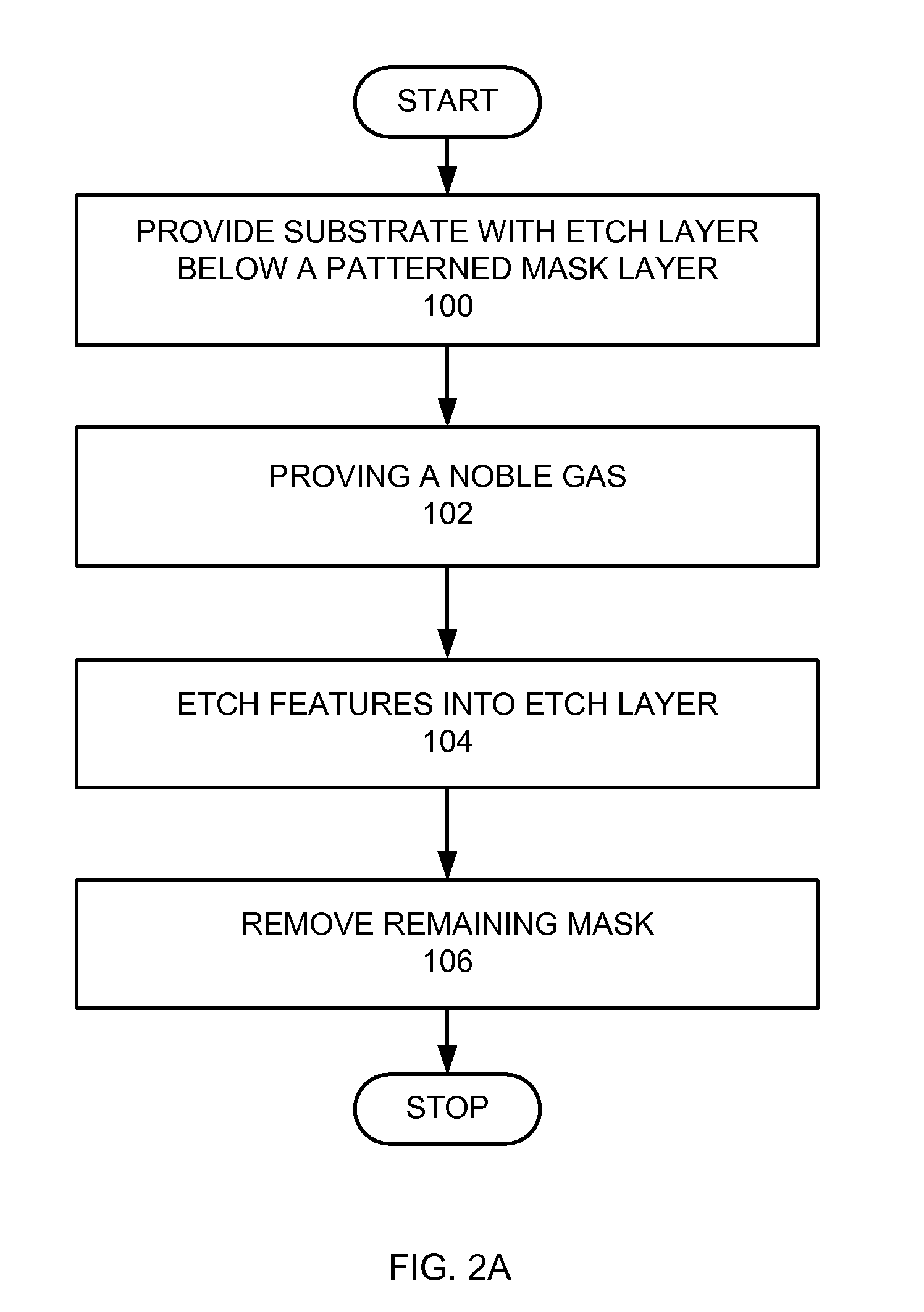
[0022]To facilitate understanding, FIG. 2A is a high-level flow chart for forming lines in a substrate. A substrate with an etch layer disposed below a patterned mask is provided (step 100). To facilitate understanding of the invention, FIG. 3 is a schematic cross-sectional view of a stack 200 of layers formed on a substrate 202, including an etch layer 204 disposed below an ARC layer 210 ...
PUM
| Property | Measurement | Unit |
|---|---|---|
| wavelength | aaaaa | aaaaa |
| wavelength | aaaaa | aaaaa |
| thickness | aaaaa | aaaaa |
Abstract
Description
Claims
Application Information