Organic electroluminescent element, organic el display device and organic el illuminating device

a technology of electroluminescent elements and display devices, applied in the direction of luminescent compositions, thermoelectric devices, chemistry apparatuses and processes, etc., can solve the problems of increasing driving voltage, low current efficiency or power efficiency, and high driving voltage, and achieve high power efficiency, low driving voltage, and high current efficiency

Active Publication Date: 2011-05-19
MITSUBISHI CHEM CORP
View PDF11 Cites 19 Cited by
  • Summary
  • Abstract
  • Description
  • Claims
  • Application Information

AI Technical Summary

Benefits of technology

[0014]The organic electroluminescent element of the present invention has a mixed layer containing a light-emitting low molecular compound and / or a charge-transporting low molecular compound in a film obtained by insolubilizing an insolubilizing polymer, whereby it has a low driving voltage, high power efficiency and high current efficiency.
[0015]Accordingly, the organic electroluminescent element of the present invention is expected to be applied to flat panel displays (for e.g. OA computers or wall-hung television sets), light sources utilizing the surface-emitting characteristics (e.g. light sources for copy machines, backlight power sources for liquid crystal displays or various meters), display panels or sign lamps, and thus, its technical value is high.

Problems solved by technology

This has been a cause of an increase of a driving voltage in an organic electroluminescent element.
For example, Patent Document 2 or 3 discloses an invention of an organic electroluminescent element wherein a hole injection layer and a light-emitting layer are formed by a wet film-forming method, but it had problems such that as compared with an element formed by a vacuum deposition method, the current efficiency or power efficiency is low, the driving voltage is high, and the luminescent efficiency is low.

Method used


Image

  • Organic electroluminescent element, organic el display device and organic el illuminating device
  • Organic electroluminescent element, organic el display device and organic el illuminating device
  • Organic electroluminescent element, organic el display device and organic el illuminating device

Examples


specific examples

[0212]Now, preferred specific examples of the eliminating polymer in the present invention will be presented, but the present invention is by no means limited thereto.

In the above formulae, n is an optional integer.

[Eliminated Film-Forming Composition]

[0213]An eliminated film is usually formed by using an eliminated film-forming composition.

[0214]In the present invention, the eliminated film-forming composition contains at least one type of the above eliminating polymer. Further, the eliminating polymer contained in the eliminated film-forming composition may contain any one type alone or different two or more types in an optional ratio and combination.

[0215]Ones other than the eliminating polymer contained in the eliminated film-forming composition are the same as those disclosed in the above section for [Cross-linked film-forming composition]. Preferred embodiments are also the same.

[Method for Forming Eliminated Film]

[0216]The method for forming the eliminated film is the same as...

example 1

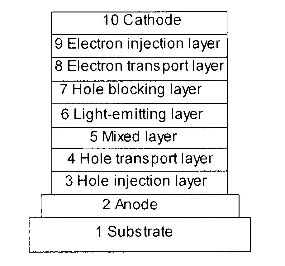
[0393]An organic electroluminescent element as shown in FIG. 1 was prepared.

[0394]An indium.tin oxide (ITO) transparent conductive film deposited in a thickness of 120 nm on a glass substrate (a sputter-deposited product, manufactured by Sanyo Vacuum Industries Co., Ltd.) was subjected to patterning in stripes with a width of 2 mm by means of a usual photolithography technique and hydrochloric acid etching to form an anode. The patterned ITO substrate was subjected to cleaning in the order of ultrasonic cleaning by an aqueous surfactant solution, water washing by ultrapure water, ultrasonic cleaning by ultrapure water and water washing by ultrapure water, then dried by compressed air and finally subjected to ultraviolet ray ozone cleaning.

[0395]Firstly, a composition for hole injection layer comprising a hole-transporting polymer compound (weight average molecular weight: 26,500, number average molecular weight: 12,000) having a repeating structure represented by the following struc...

example 2

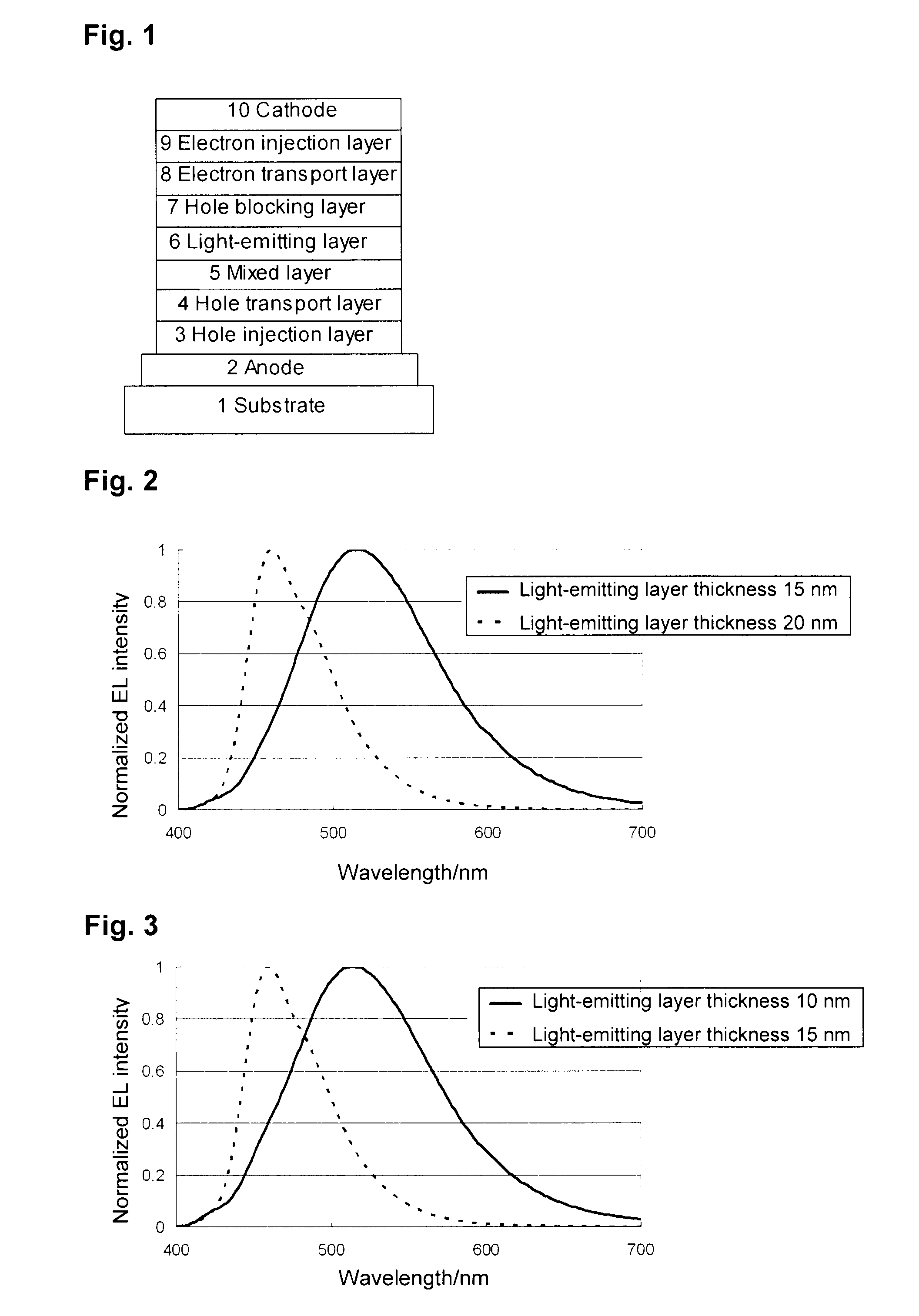
[0405]An organic electroluminescent element was prepared in the same manner as in Example 1 except that in Example 1, a light-emitting layer was formed under such a condition that the film thickness would be 20 nm when the film was formed on a glass plate, a hole blocking layer was formed in a thickness of 5 nm by using the compound (C5) represented by the following structural formula, and an electron transport layer was formed by adjusting the film thickness of Alq3 to 10 nm.

[0406]The results of measurement of the emission spectrum of this element are shown in FIG. 2. It was an organic electroluminescent element having the maximum wavelength at 460 nm.


PUM

PropertyMeasurementUnit
surface tensionaaaaaaaaaa

Abstract

To provide an organic electroluminescent element having a low driving voltage, high current efficiency and high voltage efficiency.
An organic electroluminescent element comprising an anode, a cathode and an organic layer disposed between the anode and the cathode, wherein the organic layer comprises a mixed layer containing a light-emitting low molecular compound and/or a charge-transporting low molecular compound in a film containing an insolubilized polymer obtained by insolubilizing an insolubilizing polymer, and, adjacent to the mixed layer, a layer containing a light-emitting low molecular compound and a charge-transporting low molecular compound and not containing an insolubilized polymer.

Description

TECHNICAL FIELD[0001]The present invention relates to an organic electroluminescent element, an organic EL display device and an organic EL illumination.BACKGROUND ART[0002]In recent years, developments of electroluminescent elements using organic thin films (i.e. organic electroluminescent elements) have been carried out.[0003]Among them, in order to improve the performance of an organic electroluminescent element, development of an organic electroluminescent element having a structure wherein organic thin films are laminated in a multilayer construction (hereinafter referred to as a “multilayer laminate structure”) has been actively carried out.[0004]In an organic electroluminescent element having a multilayer laminate structure, at least two layers different in composition are present. At their interface, there is a difference in the ionization potential or electron affinity, which becomes a hindrance at the time of interlayer injection of an electric charge (holes or electrons)....

Claims


Application Information

Patent Timeline
Patent Type & Authority Applications(United States)
IPC IPC(8): H01L51/54H01L51/48
CPCC08G61/12H05B33/14C08G2261/135C08G2261/141C08G2261/1424C08G2261/3162C08L65/00C08L79/02C09K11/06C09K2211/1433H01L51/0035H01L51/0043H01L51/0058H01L51/006H01L51/0067H01L51/008H01L51/0081H01L51/5012H01L51/5048C08G73/026H10K85/111H10K85/151H10K85/626H10K85/633H10K85/654H10K85/322H10K85/324H10K50/14H10K50/11
Inventor OKABE, KAZUKITAKAHASHI, ATSUSHIABE, TOMOHIROTSURUTANI, YASUYUKISATO, HIDEKI
Owner MITSUBISHI CHEM CORP
Why Eureka
Try Eureka