Semiconductor device

a technology of semiconductors and devices, applied in the field of semiconductor devices, can solve the problems of difficult melting of silicon carbide, inability to manufacture silicon carbide by a high-productivity method, and defects called micropipes of silicon carbide, so as to achieve favorable operation, reduce the concentration of hydrogen, and increase the purity

Inactive Publication Date: 2011-05-26
SEMICON ENERGY LAB CO LTD
View PDF21 Cites 55 Cited by
  • Summary
  • Abstract
  • Description
  • Claims
  • Application Information

AI Technical Summary

Benefits of technology

[0018]With one embodiment of the present invention including an oxide semiconductor in which the hydrogen concentration is reduced and the purity is increased, a transistor can be favorably operated. In particular, the withstand voltage can be increased, a short-channel effect can be suppressed, and an on / off ratio can be increased. Thus, with use of the transistor, a semiconductor device for high power application can be manufactured.

Problems solved by technology

However, it is difficult to melt silicon carbide because of its characteristics; therefore, silicon carbide cannot be manufactured by a method having high productivity such as a Czochralski (CZ) method or the like which is used for manufacturing a silicon wafer.
Moreover, there is also a problem in that silicon carbide has defects called micropipes.
Owing to these problems, commercialization of a semiconductor device using silicon carbide is delayed.

Method used


Image

  • Semiconductor device
  • Semiconductor device
  • Semiconductor device

Examples


embodiment 1

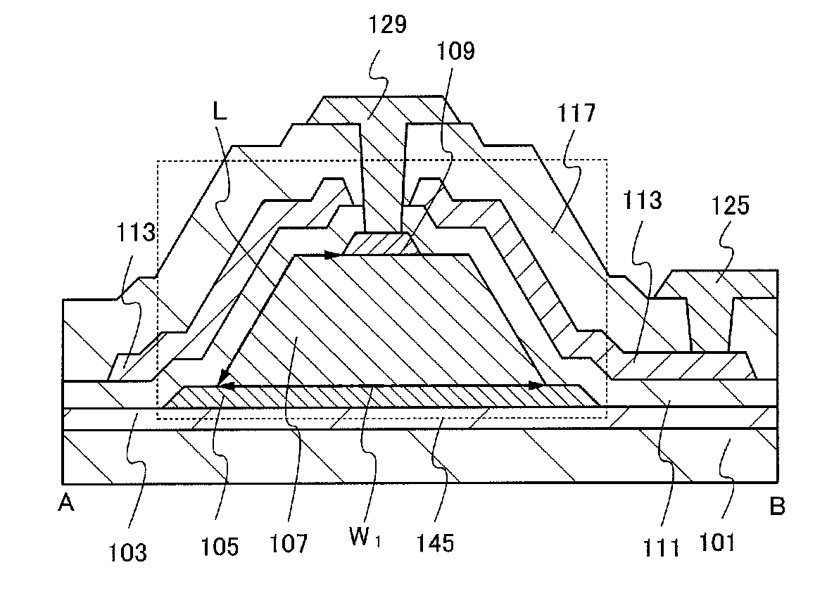
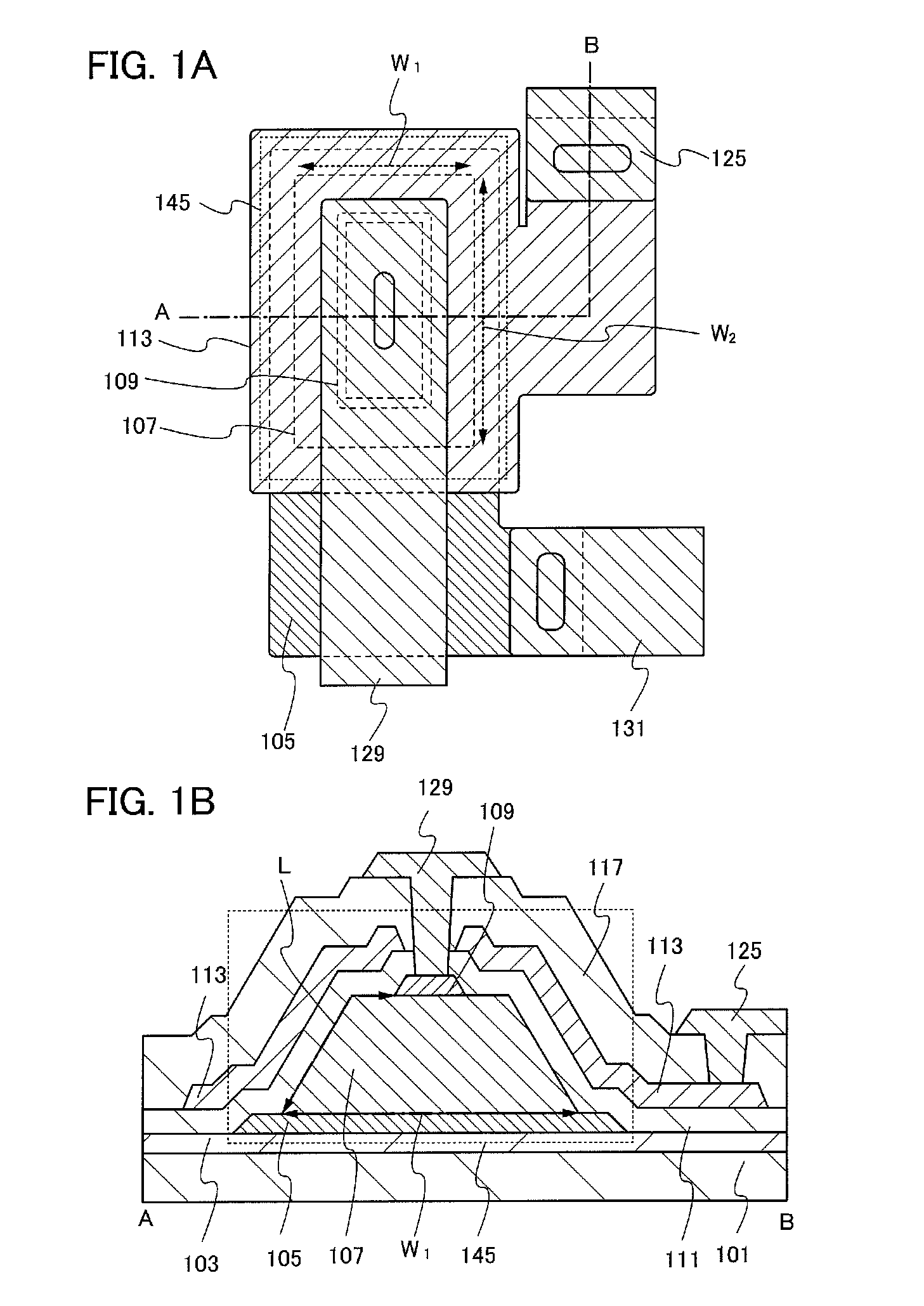
[0046]In this embodiment, a structure of a transistor will be described with reference to FIGS. 1A and 1B.

[0047]FIG. 1A is a top view of a transistor 145, and FIG. 1B corresponds to a cross-sectional view taken along dashed line A-B in FIG. 1A.

[0048]As illustrated in FIG. 1B, a first electrode 105, an oxide semiconductor film 107, and a second electrode 109 are stacked over an insulating film 103 formed over a substrate 101. Note that end portions of the second electrode 109 are positioned inside end portions of the oxide semiconductor film 107. A gate insulating film 111 is provided so as to cover the first electrode 105, the oxide semiconductor film 107, and the second electrode 109. Over the gate insulating film 111, a third electrode 113 is formed so as to face at least side surfaces of the oxide semiconductor film and the second electrode. An insulating film 117 functioning as an interlayer insulating film is provided over the gate insulating film 111 and the third electrode 11...

embodiment 2

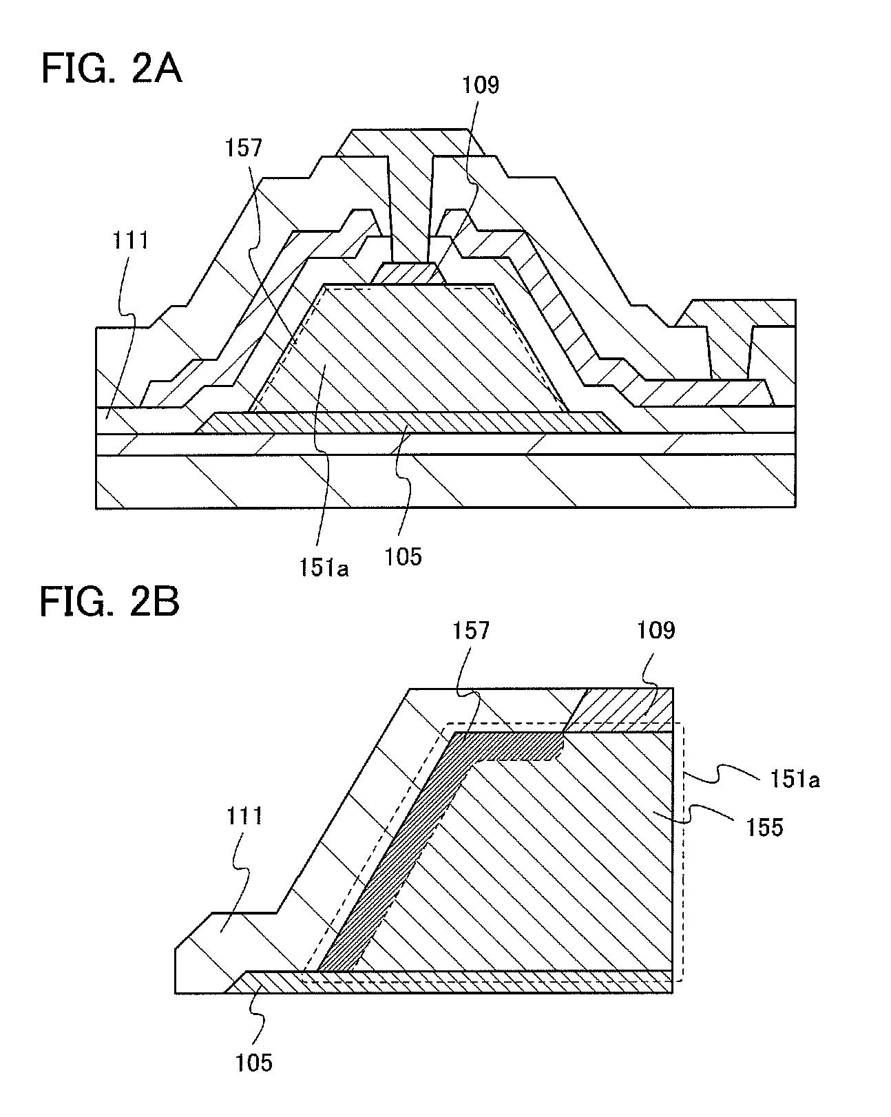
[0119]In this embodiment, a structure of a transistor with higher reliability and higher field-effect mobility than those in Embodiment 1 will be described with reference to FIGS. 2A and 2B and FIG. 3.

[0120]In this embodiment, an oxide semiconductor film 151a which is provided between a first electrode 105 and a second electrode 109 as illustrated in FIG. 2A includes a crystal region 157 in a superficial portion that is in contact with a gate insulating film 111. An enlarged view of the vicinity of the interface between the oxide semiconductor film 151a and the gate insulating film 111 is illustrated in FIG. 2B.

[0121]The oxide semiconductor film 151a includes an amorphous region 155 which mainly contains an amorphous oxide semiconductor and the crystal region 157 formed in the superficial portion of the oxide semiconductor film 151a. Note that the superficial portion indicates a region that is located at a distance (depth) from the top surface of 10% or less of the thickness of the ...

embodiment 3

[0133]In this embodiment, a structure of a transistor with higher reliability and higher field-effect mobility than those in Embodiment 1 will be described with reference to FIGS. 4A to 4C.

[0134]In this embodiment, an oxide semiconductor film which is provided between a first electrode 105 and a second electrode 109 as illustrated in FIG. 4A includes a crystal region 157 in a superficial portion that is in contact with a gate insulating film 111 and a second electrode 109. An enlarged view of the vicinity of oxide semiconductor films 151b and 151c is illustrated in FIGS. 4B and 4C.

[0135]In FIG. 4B, the oxide semiconductor film 151b includes a crystal region 157 in a superficial portion that is in contact with the gate insulating film 111 and the second electrode 109.

[0136]In FIG. 4C, the oxide semiconductor film 151c includes a crystal region 157 in a region that is in contact with the gate insulating film 111 and a region that is apart from the second electrode 109 at a certain dis...


PUM


Abstract

Provided is a semiconductor device for high power application including a novel semiconductor material with high productivity. Alternatively, provided is a semiconductor device having a novel structure in which the novel semiconductor material is used. Provided is a vertical transistor including a channel formation region formed using an oxide semiconductor which has a wider band gap than a silicon semiconductor and is an intrinsic semiconductor or a substantially intrinsic semiconductor with impurities that can serve as electron donors (donors) in the oxide semiconductor removed. The thickness of the oxide semiconductor is greater than or equal to 1 μm, preferably greater than 3 μm, more preferably greater than or equal to 10 μm, and end portions of one of electrodes that are in contact with the oxide semiconductor is placed inside end portions of the oxide semiconductor.

Description

TECHNICAL FIELD[0001]The technical field of the disclosed invention relates to transistors each including an oxide semiconductor and semiconductor devices each including any of the transistors.BACKGROUND ART[0002]A technique for forming a thin film transistor (TFT) by using a thin semiconductor film formed over a substrate having an insulating surface has attracted attention. A thin film transistor is used for a display device typified by a liquid crystal television. A silicon-based semiconductor material is known as a material for a thin semiconductor film that can be applied to a thin film transistor, and in addition, an oxide semiconductor has attracted attention as another material that can be applied to a thin film transistor.[0003]As a material of the oxide semiconductor, zinc oxide or a material containing zinc oxide as its component is known. Further, a thin film transistor formed using an amorphous oxide (an oxide semiconductor) having an electron carrier density of lower t...

Claims


Application Information

Patent Timeline
Patent Type & Authority Applications(United States)
IPC IPC(8): H01L29/78
CPCH01L27/1225H01L29/42392H01L29/78696H01L29/78642H01L29/7869H01L29/78606H01L29/06
Inventor YAMAZAKI, SHUNPEIKAWAE, DAISUKE
Owner SEMICON ENERGY LAB CO LTD
Why Eureka
Try Eureka