Display device

Active Publication Date: 2011-06-09
SEMICON ENERGY LAB CO LTD
View PDF99 Cites 31 Cited by
  • Summary
  • Abstract
  • Description
  • Claims
  • Application Information

AI Technical Summary

Benefits of technology

[0045]The above structure and advantageous effects can be obtained when the transistor 101 is formed using an intrinsic or substantially intrinsic oxide semiconductor and the off-state current of the transistor 101 is 1×10⁻¹⁷ A/μm or less.
[0046]In contrast, a conventional oxide semiconductor has n-type conductivity and an off-state current of about 1×10⁻⁹ A/μm at the minimum. Therefore, a capacitor in a pixel is essential, and the time taken to write a signal is long.
[0047]Here, the conducting mechanism of a transistor including an oxide semiconductor in this embodiment is described with reference to FIG. 5, FIG. 6, FIGS. 7A and 7B, and FIGS. 8A and 8B. Note that the following description is based on the assumption of an ideal situation for easy understanding and does not necessarily reflect a real situation. Further, the following description is just a consideration and does not influence the validity of the present invention.
[0048]FIG. 5 illustrates a relationship between a vacuum level, the work function (φM) of a metal (Metal), and the electron affinity (χ) of an oxide semiconductor (OS).

Problems solved by technology

Thus, considering a time constant τ=R(CLC+CS) which is necessary for storing electric charge, there is a problem in that it takes a longer time to write a signal by the time taken to store the storage capacitance CS.
However, due to the time taken to store electric charge in a capacitor, the time taken to reach

Method used


Image

  • Display device
  • Display device
  • Display device

Examples


embodiment 1

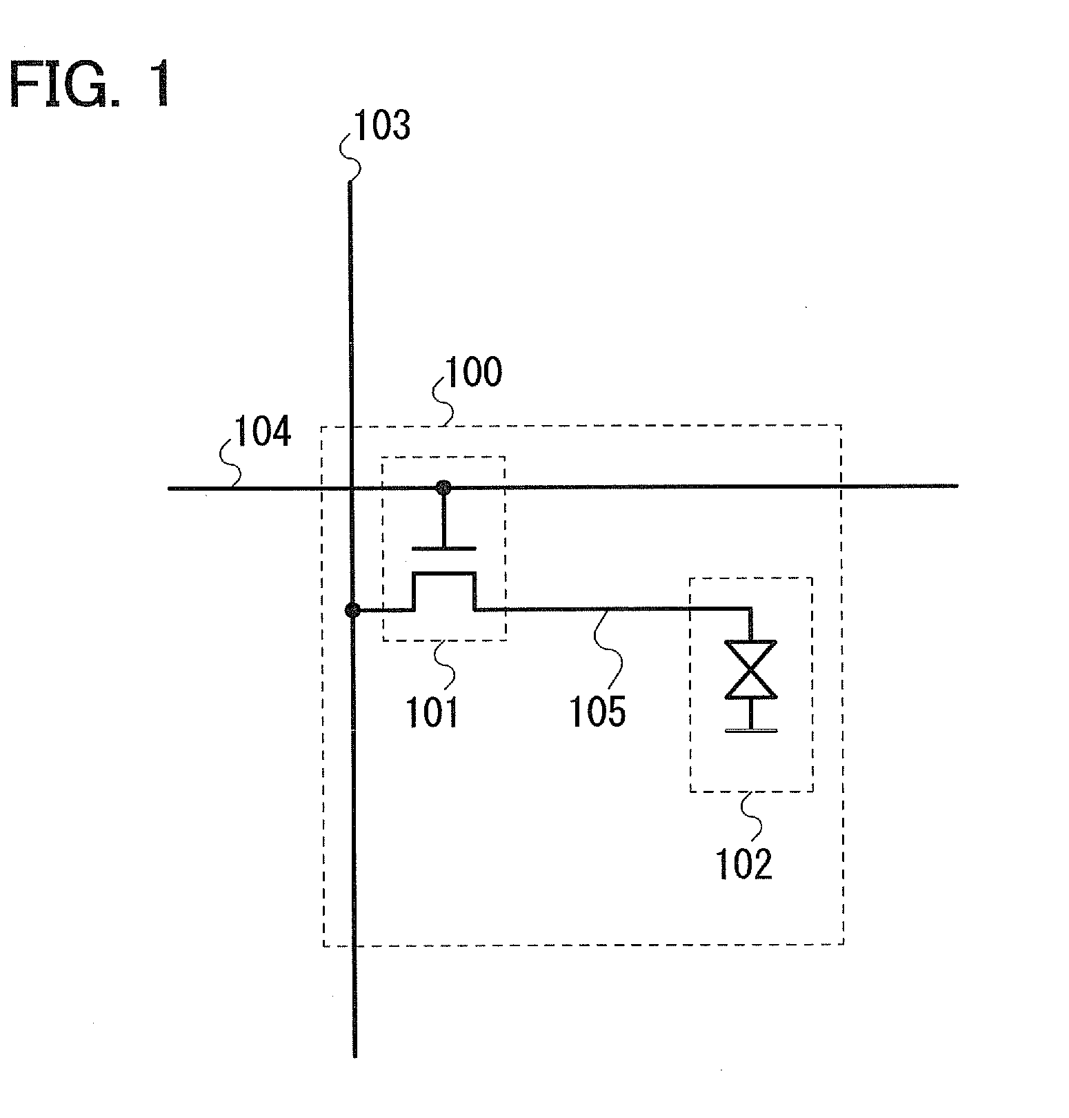
[0035]An example of a pixel in a liquid crystal display device is described with reference to FIG. 1. Elements included in a pixel 100 are a transistor 101 which functions as a switch element and a liquid crystal element 102.

[0036]A gate of the transistor 101 is electrically connected to a wiring 103 (a gate signal line). One of a source and a drain of the transistor 101 is electrically connected to a wiring 104 (a source signal line). The other is electrically connected to the liquid crystal element 102.

[0037]In this embodiment, an intrinsic or substantially intrinsic oxide semiconductor is used as the semiconductor material of the transistor 101, and the off-state current per micrometer of the channel width of the transistor 101 is 1×10⁻¹⁷ A or less (1×10⁻¹⁷ A / μm or less).

[0038]When the off-state current of the transistor 101 is 1×10⁻¹⁷ A / μm or less, it means that the amount of leakage current is substantially zero when the transistor 101 is off. In other words, the potential of a...

embodiment 2

[0072]In this embodiment, the case where an FFS mode is used as the display method of a liquid crystal display device is described.

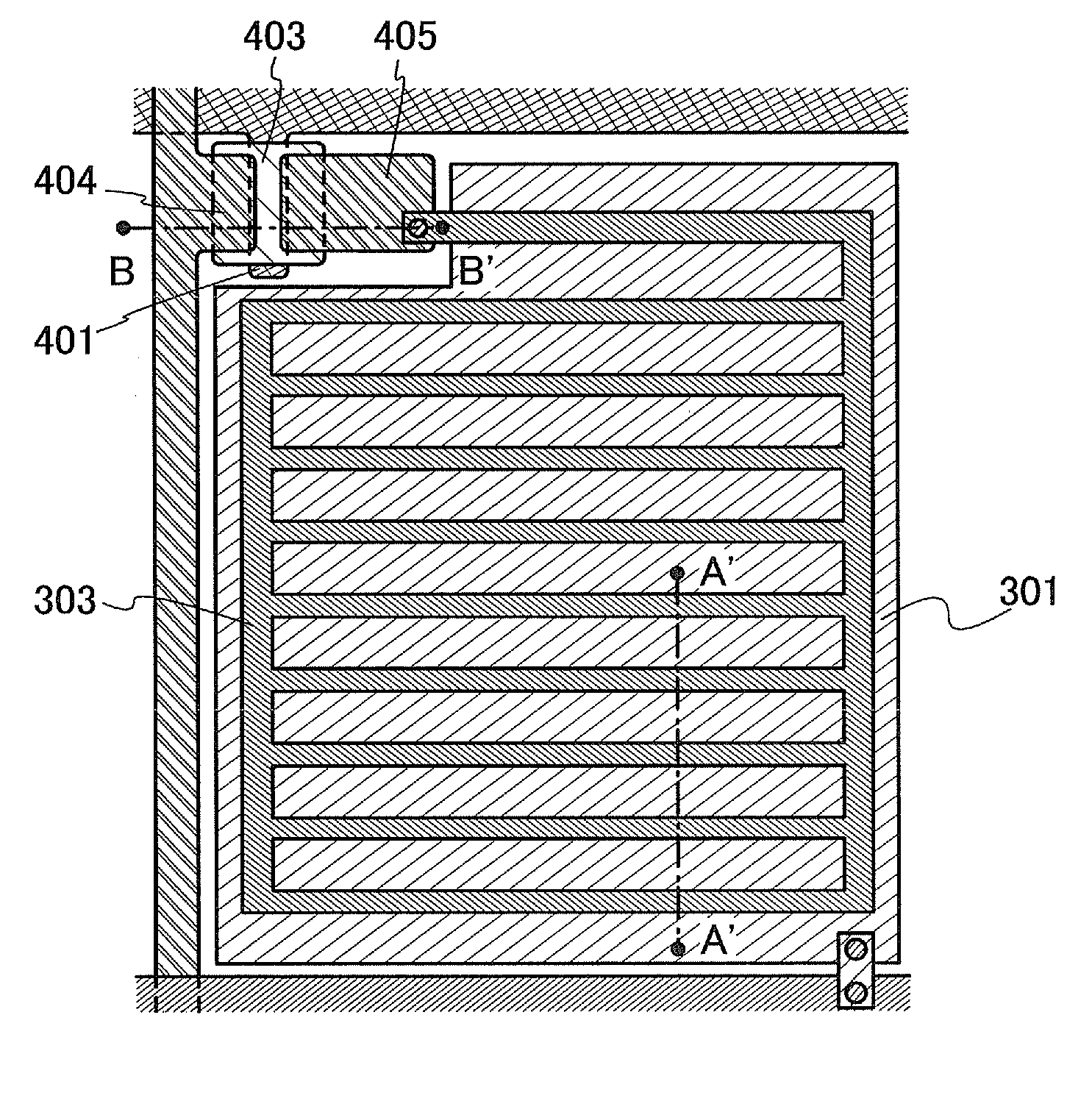
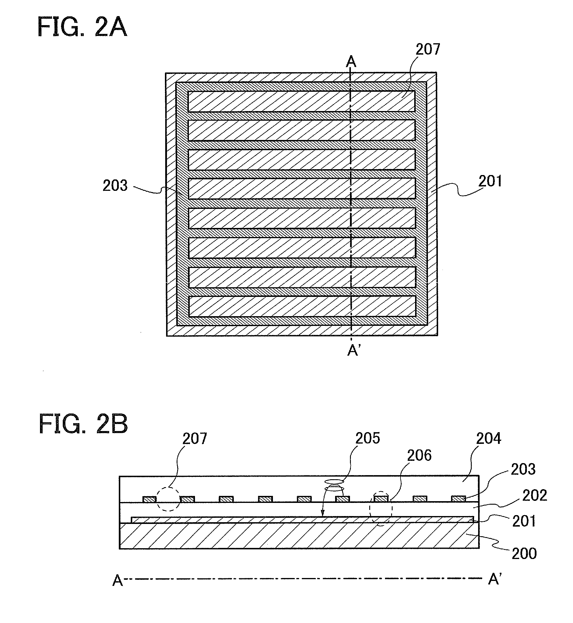
[0073]First, FIGS. 2A and 2B illustrate an example of an electrode structure in a pixel with a conventional FFS mode. In FIGS. 2A and 2B, the liquid crystal element 5002 in the pixel circuit in FIG. 13 is illustrated. FIG. 2A is a top view and FIG. 2B is a cross-sectional view.

[0074]In FIGS. 2A and 2B, an electrode 201 is formed over a substrate 200; an insulating film 202 is formed so as to cover the electrode 201; an electrode 203 is formed over the insulating film 202; and a liquid crystal layer 204 is formed over the electrode 203. One of the electrode 201 and the electrode 203 is a pixel electrode. The other is a common electrode. The electrode 203 has a slit 207 (an opening portion). The electrode 201 is a plate-like (a shape covering the entire surface) electrode. The insulating film 202 may be a single layer or a stacked layer.

[0075]When a horizo...

embodiment 3

[0093]In this embodiment, an example of a method for manufacturing a semiconductor device is described with reference to FIGS. 9A to 9E.

[0094]First, after a conductive film is formed over a substrate 1000 having an insulating surface, a gate electrode 1001 is formed in a first photolithography process. End portions of the gate electrode 1001 are preferably tapered because coverage with a gate insulating film stacked thereover is improved.

[0095]Although there is no particular limitation on a substrate which can be used as the substrate 1000 having an insulating surface, it is necessary that the substrate have at least heat resistance high enough to withstand heat treatment to be performed later. For example, various kinds of glass substrates can be used.

[0096]In the case where the temperature of the heat treatment to be performed later is high, a substrate whose strain point is higher than or equal to 730° C. is preferably used as a glass substrate. For the glass substrate, for examp...


PUM


Abstract

The time taken to write a signal to a pixel is shortened in a display device. Further, a signal is written at high speed even when high voltage is applied. The display device includes a pixel including a transistor and a liquid crystal element electrically connected to a source or a drain of the transistor. The transistor includes an intrinsic or substantially intrinsic oxide semiconductor as a semiconductor material and has an off-state current of 1×10⁻¹⁷ A/μm or less. The pixel does not include a capacitor. Since it is not necessary to provide a capacitor, the time taken to write a signal can be shortened.

Description

TECHNICAL FIELD[0001]The technical field of the present invention relates to a semiconductor device and a manufacturing method thereof. Further, the technical field of the present invention relates to a display device including the semiconductor device and a driving method thereof.BACKGROUND ART[0002]As liquid crystal display devices, active matrix liquid crystal display devices in which pixels include switch elements are widely used. As illustrated in FIG. 13, a pixel 5000 includes a transistor 5001 which functions as a switch element, a liquid crystal element 5002 to which a video signal is input from a wiring 5004 through the transistor 5001, and a capacitor element 5003 which holds the video signal written to the liquid crystal element 5002. With provision of the capacitor element 5003, a video signal can be held even when the switch element is off.[0003]Silicon, which has broad utility, is used as the semiconductor material of a transistor. However, in recent years, not only br...

Claims


Application Information

Patent Timeline
IPC IPC(8): H04N3/14G02F1/136
CPCG09G3/3696G02F1/1368H01L27/1225
Inventor YAMAZAKI, SHUNPEIKIMURA, HAJIME
Owner SEMICON ENERGY LAB CO LTD
Why Eureka
Try Eureka