Low-Noise High Efficiency Bias Generation Circuits and Method

a bias generation and low-noise technology, applied in the field of electronic integrated circuits, can solve the problems of undesired emissions, inconvenient supply of additional supplies, and long coupling between conductors such external supplies and the i

Active Publication Date: 2011-06-30
PSEMI CORP
View PDF99 Cites 73 Cited by
  • Summary
  • Abstract
  • Description
  • Claims
  • Application Information

AI Technical Summary

Benefits of technology

[0015]As an aid to biasing capacitively coupled control signals to the transfer capacitor switching devices, it may be helpful to employ active bias “resistors,” active circuits that couple a bias voltage on a first node to a second node coupled to a transistor control node. A goal is to couple the first node bias voltage to the second node without unduly reducing the amplitude of an alternating drive signal also applied to the second node, which drive signal may be oscillating and may moreover be substantially sine-like. Embodiments of such active bias-coupling circuits may be configured to substantially reduce, compared to the voltage between the two nodes, a voltage appearing across an impedance limiting current between the two nodes, or alternatively may entirely avoid the presence of significant resistors and limit current conduction by capacitive charging, with further current through active devices as may be suitable. They may also substantially preclude

Problems solved by technology

Such different supplies can be provided externally to the integrated circuit, but this is undesirable from a user standpoint.
Providing additional supplies is not only inconvenient for the user, but may also cause the conductors coupling such external supplies to the IC to be unduly long, which among other difficulties may cause undesired emissions if noise is present on the supply.
However, charge pumps have characteristics that have rendered them difficult to use in certain applications.
In particular, charge pumps have invariably created a substantial amount of electrical noise.
In some applications the noise generated by a charge pump may cause the IC or system in which such IC is disposed to exceed such maximum permitted noise emissions.
Many of the products that employ RF switches are transceivers, such as cell pho

Method used


Image

  • Low-Noise High Efficiency Bias Generation Circuits and Method
  • Low-Noise High Efficiency Bias Generation Circuits and Method
  • Low-Noise High Efficiency Bias Generation Circuits and Method

Examples


Embodiment Construction

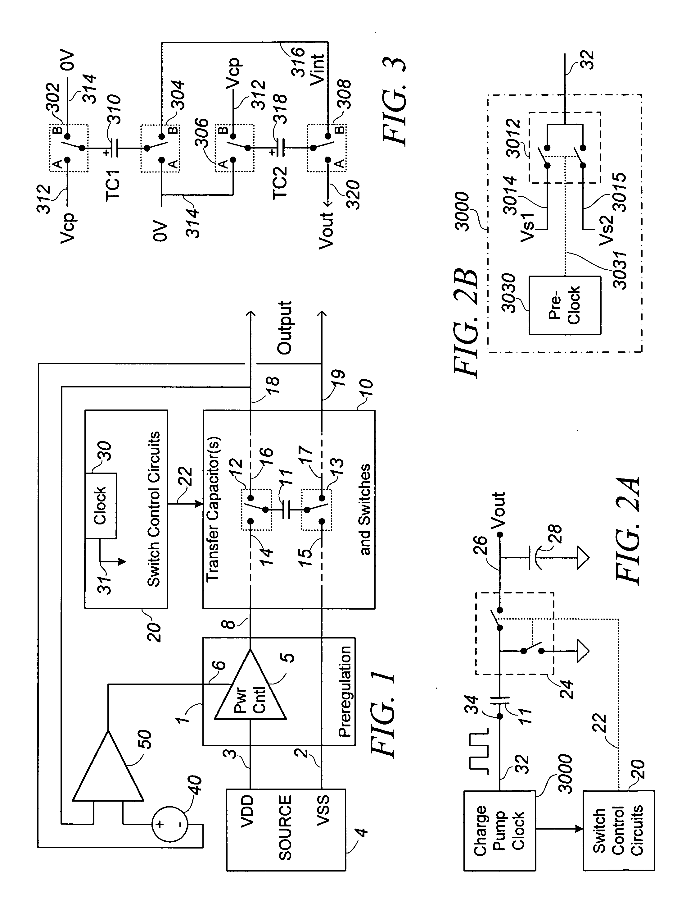
[0036]The bias generation circuits described herein are fabricated on integrated circuits, providing bias and other supply voltages. A bias generation method or apparatus may employ one or more charge pumps to develop bias voltages. Charge pumps, as that term is used herein, are defined by a process of storing charge from an input supply on a transfer capacitor, then switching the nodes to which the transfer capacitor is coupled so as to transfer some portion of that stored charge to an output supply. The charge pumps described are expected to be entirely within a single monolithic integrated circuit, except perhaps for filtering components such as external capacitors.

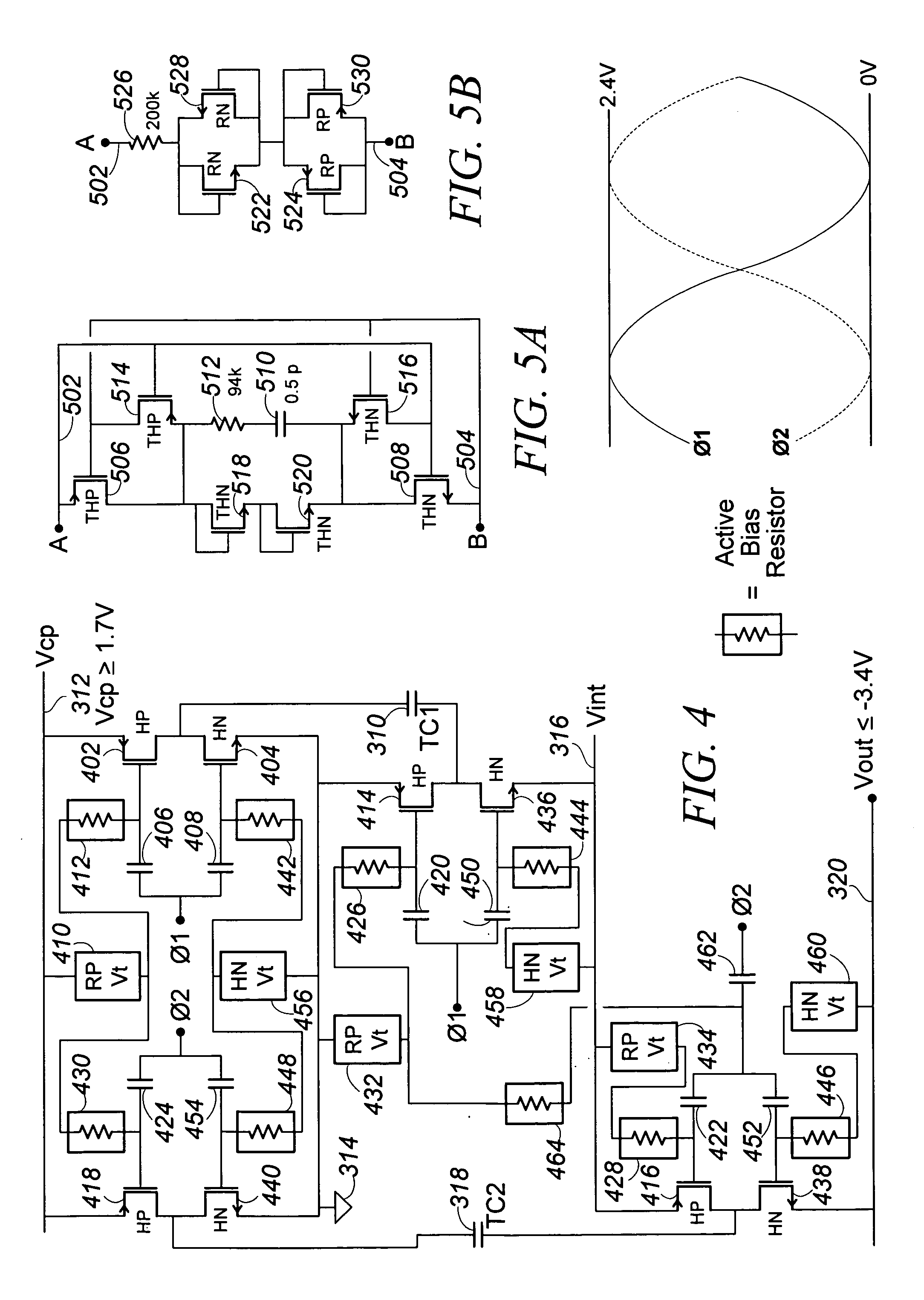
[0037]As was developed in the related U.S. patent application Ser. No. 10 / 658,154 filed Sep. 8, 2003, entitled “Low Noise Charge Pump Method and Apparatus” and incorporated herein by reference, a sinusoidal or sine-like charge pump clock output can reduce harmonic noise generation by the charge pump, particularly if th...


PUM


Abstract

A bias generation method or apparatus defined by any one or any practical combination of numerous features that contribute to low noise and/or high efficiency biasing, including: having a charge pump control clock output with a waveform having limited harmonic content or distortion compared to a sine wave; having a ring oscillator to generating a charge pump clock that includes inverters current limited by cascode devices and achieves substantially rail-to-rail output amplitude; having a differential ring oscillator with optional startup and/or phase locking features to produce two phase outputs suitably matched and in adequate phase opposition; having a ring oscillator of less than five stages generating a charge pump clock; capacitively coupling the clock output(s) to some or all of the charge transfer capacitor switches; biasing an FET, which is capacitively coupled to a drive signal, to a bias voltage via an “active bias resistor” circuit that conducts between output terminals only during portions of a waveform appearing between the terminals, and/or wherein the bias voltage is generated by switching a small capacitance at cycles of said waveform. A charge pump for the bias generation may include a regulating feed back loop including an OTA that is also suitable for other uses, the OTA having a ratio-control input that controls a current mirror ratio in a differential amplifier over a continuous range, and optionally has differential outputs including an inverting output produced by a second differential amplifier that optionally includes a variable ratio current mirror controlled by the same ratio-control input. The ratio-control input may therefore control a common mode voltage of the differential outputs of the OTA. A control loop around the OTA may be configured to control the ratio of one or more variable ratio current mirrors, which may particularly control the output common mode voltage, and may control it such that the inverting output level tracks the non-inverting output level to cause the amplifier to function as a high-gain integrator.

Description

[0001]This application claims priority to U.S. application No. 61 / 135,279 filed Jul. 18, 2008 and entitled “Low Noise Charge Pump with Common-Mode Tuning Op Amp”, attorney docket number PER-027-PROV-1, the entire contents of which are hereby incorporated by reference herein, and hereby incorporates by reference the entire contents of U.S. patent application Ser. No. 10 / 658,154 filed Sep. 8, 2003 and entitled “Low Noise Charge Pump Method and Apparatus”.BACKGROUND[0002]1. Field[0003]The present disclosure is widely applicable to electronic integrated circuits (“ICs”).[0004]2. Related Art[0005]It is usually desirable for an IC to operate from a single voltage supply. However, many ICs require two or more different voltage supplies, for example to provide internal bias supplies, for ideal operation. Such different supplies can be provided externally to the integrated circuit, but this is undesirable from a user standpoint. Providing additional supplies is not only inconvenient for the ...

Claims


Application Information

Patent Timeline
IPC IPC(8): H03F3/04G05F3/16G05F3/08
CPCH02M3/07H03H11/245H03F3/45183H03F3/45237H03F3/45475H03F3/45659H03F2200/453H03F2200/456H03F2200/474H03F2203/45138H03F2203/45188H03F2203/45366H03F2203/45418H03F2203/45424H03F2203/45471H03F2203/45642H03K17/145H03F1/26
Inventor KIM, TAE YOUNENGLEKIRK, ROBERT MARKKELLY, DYLAN J.
Owner PSEMI CORP
Why Eureka
Try Eureka