

Method of forming a dielectric layer and method of manufacturing a semiconductor device using the same
- Summary
- Abstract
- Description
- Claims
- Application Information
AI Technical Summary
Benefits of technology
Problems solved by technology
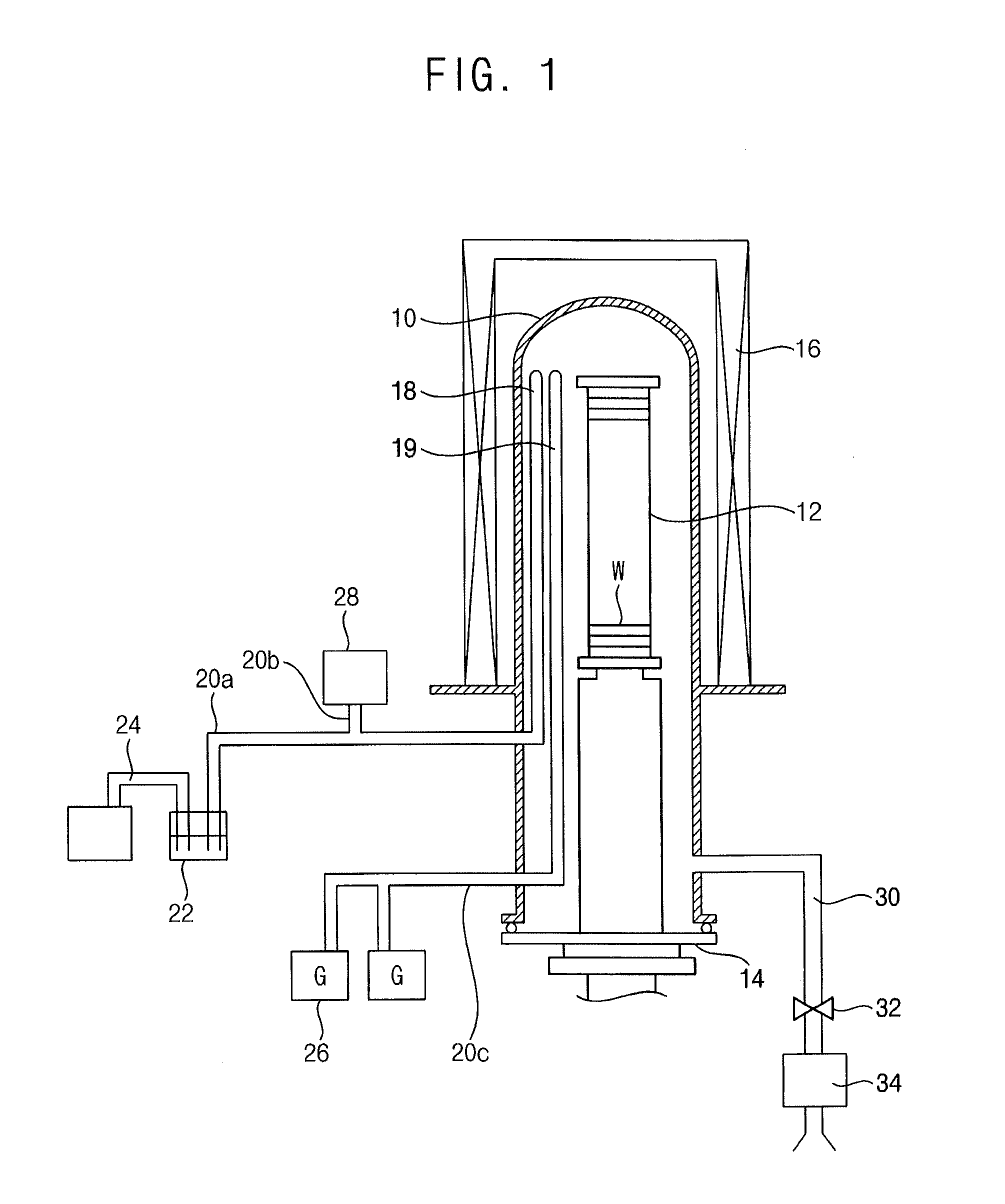
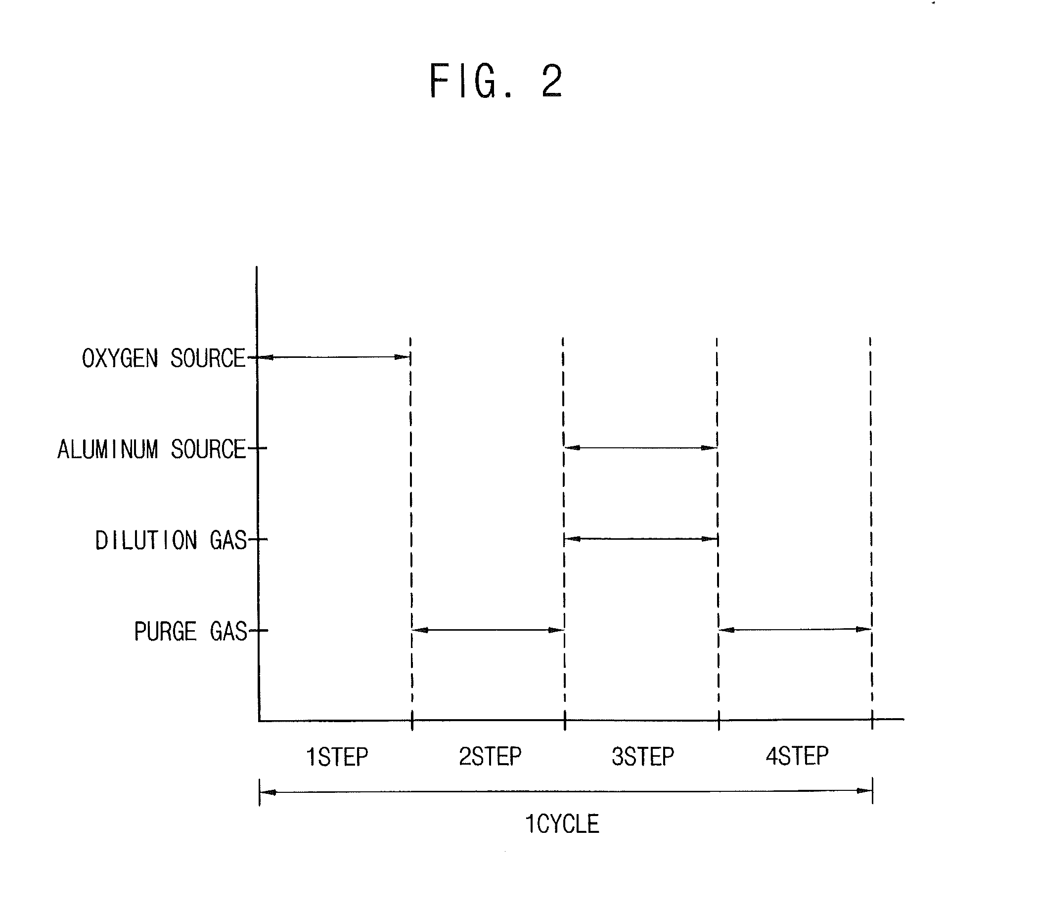
Method used
Image

Examples
embodiment 1
[0096]Hereinafter, a flash memory device including the aluminum oxide layer that is illustrated with reference to FIGS. 1 and 2 and a method of manufacturing the flash memory device will be explained in detail.
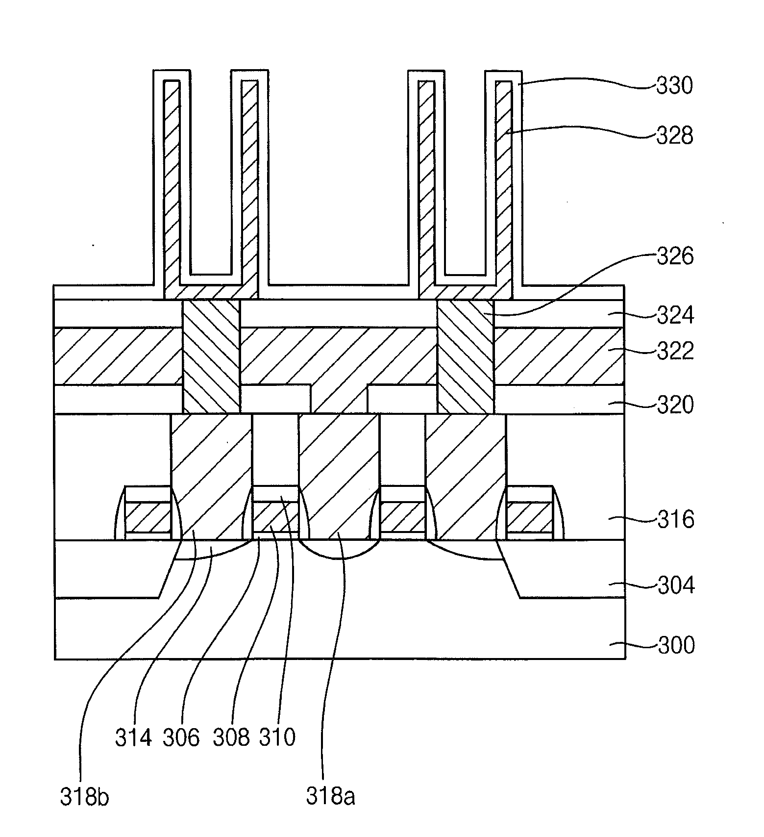
[0097]FIG. 3 is a plan view illustrating a flash memory device in accordance with a first example embodiment. FIG. 4 is a cross-sectional view illustrating the flash memory device in FIG. 3. FIG. 4 is a cross-sectional view taken along the line I-I′ and the line II-II′ in FIG. 3.
[0098]Referring to FIGS. 3 and 4, a substrate 100 having an isolation layer pattern 108 may be provided. The isolation layer pattern may define an active region in the substrate 100. The active region may have a linear shape extending a first direction.
[0099]A tunnel oxide layer 102 and a floating gate pattern 104a may be provided on the substrate 100. The tunnel oxide layer 102 may include silicon oxide. The floating gate pattern 104a may include polysilicon doped with impurities.
[0100]A dielectric la...
embodiment 2
[0118]FIG. 9 is a cross-sectional view illustrating a flash memory device in accordance with a second example embodiment. The flash memory device of this embodiment includes the aluminum oxide layer that is illustrated with reference to FIGS. 1 and 2. The flash memory device of this embodiment is substantially the same as in Embodiment 1 except that a charge trapping layer is used for trapping electric charges.
[0119]Referring to FIG. 9, a substrate 100 having an isolation layer pattern (not illustrated) may be provided. A tunnel oxide layer 102, a charge trapping layer pattern 130a and a dielectric layer pattern 110a may be provided on the substrate 100.
[0120]The charge trapping layer pattern 130a may include silicon nitride. Alternatively, the charge trapping layer pattern 130a may include metal oxide.
[0121]The dielectric layer pattern 110a may include aluminum oxide. The aluminum oxide may be formed by the method illustrated with reference to FIGS. 1 and 2. Accordingly, the alumin...
embodiment 3
[0124]FIG. 10A is a perspective view illustrating a vertical-type NAND flash memory device in accordance with a third example embodiment. FIG. 10B is a cross-sectional view illustrating the vertical-type NAND flash memory device of FIG. 10A.
[0125]The vertical-type NAND flash memory device of this embodiment includes the aluminum oxide layer that is illustrated with reference to FIGS. 1 and 2.
[0126]Referring to FIGS. 10A and 10B, a substrate 200 including a single-crystalline semiconductor material may be provided. An impurity region (not illustrated) may be provided under a surface of the substrate 200 to be provided as a common source line. The impurity region may be connected to a lower portion of each of cell strings that is formed in a single-crystalline semiconductor pattern 212a.
[0127]A pad oxide layer 202 may be provided on the substrate 200. Insulation layer patterns 214 may be provided on the substrate 200. The insulation layer pattern 214 may have a linear shape extending...
PUM
| Property | Measurement | Unit |
|---|---|---|
| Temperature | aaaaa | aaaaa |
| Temperature | aaaaa | aaaaa |
| Concentration | aaaaa | aaaaa |
Abstract
Description
Claims
Application Information