Back side illumination image sensor and a process thereof

a back side illumination and image sensor technology, applied in the field of image sensors, can solve the problems of difficult to have a large margin on the second overlap, complicating process optimization, and inability to precisely control, so as to improve the overlap, reduce the surface dark current, and improve the accumulation of holes

Active Publication Date: 2011-07-14
HIMAX IMAGING LIMITED
View PDF3 Cites 8 Cited by
  • Summary
  • Abstract
  • Description
  • Claims
  • Application Information

AI Technical Summary

Benefits of technology

[0011]In view of the foregoing, it is an object of the embodiment of the present invention to provide a process and structure of a non-SA back side illumination (BSI) CMOS image sensor (CIS) that may increase the overlap between the n-type implant and the transfer gate. In one embodiment, an extended transfer gate is formed to improve hole accumulation with off transfer gate, thereby reducing surface dark current. Moreover, if non-SA BSI CIS is applied to the advanced three dimensional (3D) CIS structure, the coupling capacitance between a transfer-gate via and a floating-diffusion via may be substantially reduced, thereby reducing the coupling capacitance between them and thus increasing conversion gain. Further, BSI red response may be boosted by forming reflection layers by the extended transfer gate poly on top of PD.

Problems solved by technology

One of the disadvantages of the non-SA FSI CIS is the overlap issue, in which the first overlap 100 between the p-type implant 10 and the transfer gate (Tx) 14 and the second overlap 120 between the n-type implant 12 and the transfer gate 14 cannot be precisely controlled.
However, it is difficult to have a large margin on the second overlap 120 between the n-type implant 12 and the transfer gate 14 due to some design constrains such as the photodiode depth, shape, blue response or transfer gate height.
Accordingly, the tiny second overlap 120 may be easily affected by other implants, particularly when the pixel size is very small, thereby complicating the process optimization.
However, according to this scheme, the effective area (or optical fill factor) for receiving incoming light becomes smaller, thereby degrading quantum efficiency (QE).

Method used


Image

  • Back side illumination image sensor and a process thereof
  • Back side illumination image sensor and a process thereof
  • Back side illumination image sensor and a process thereof

Examples


first embodiment

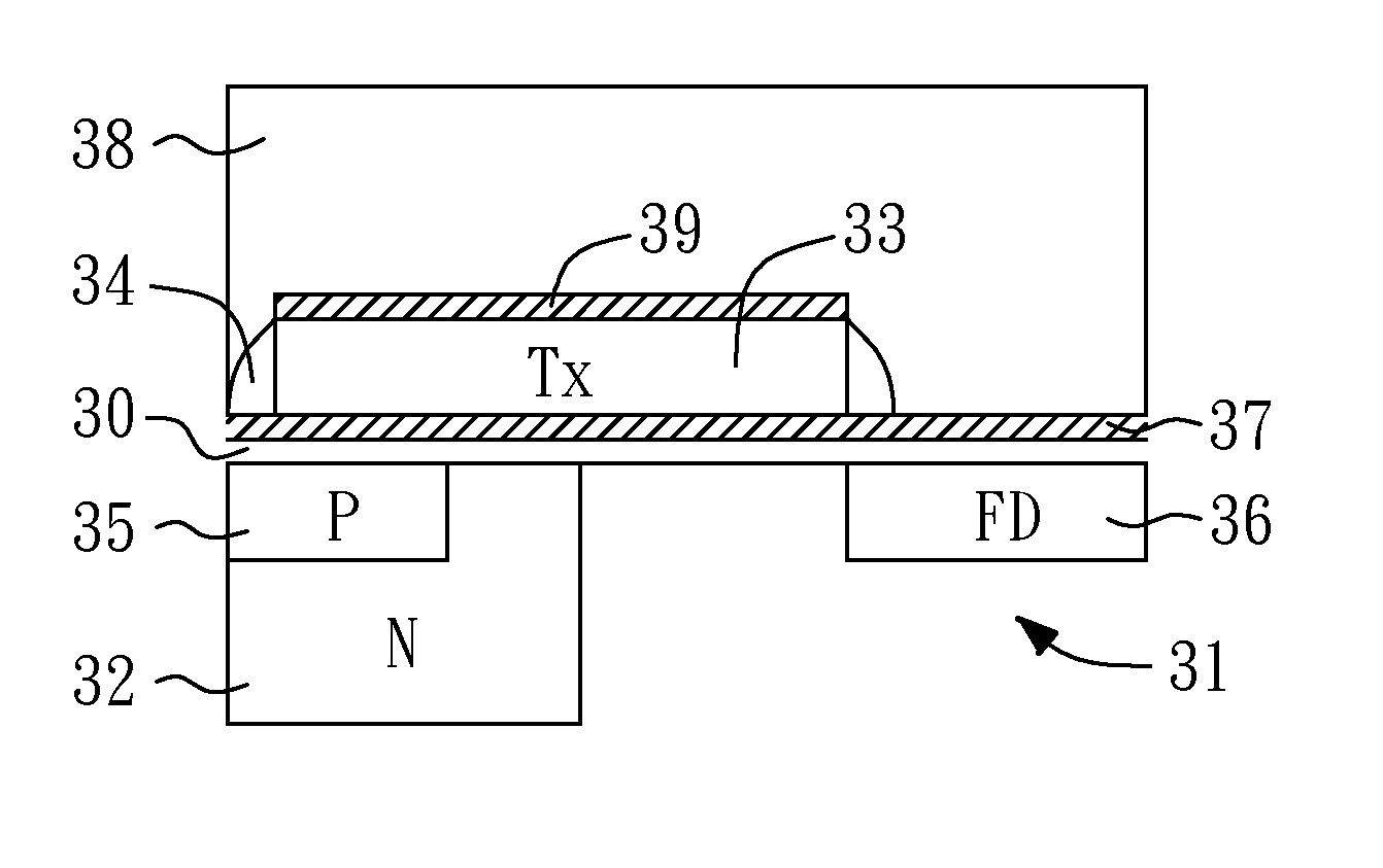
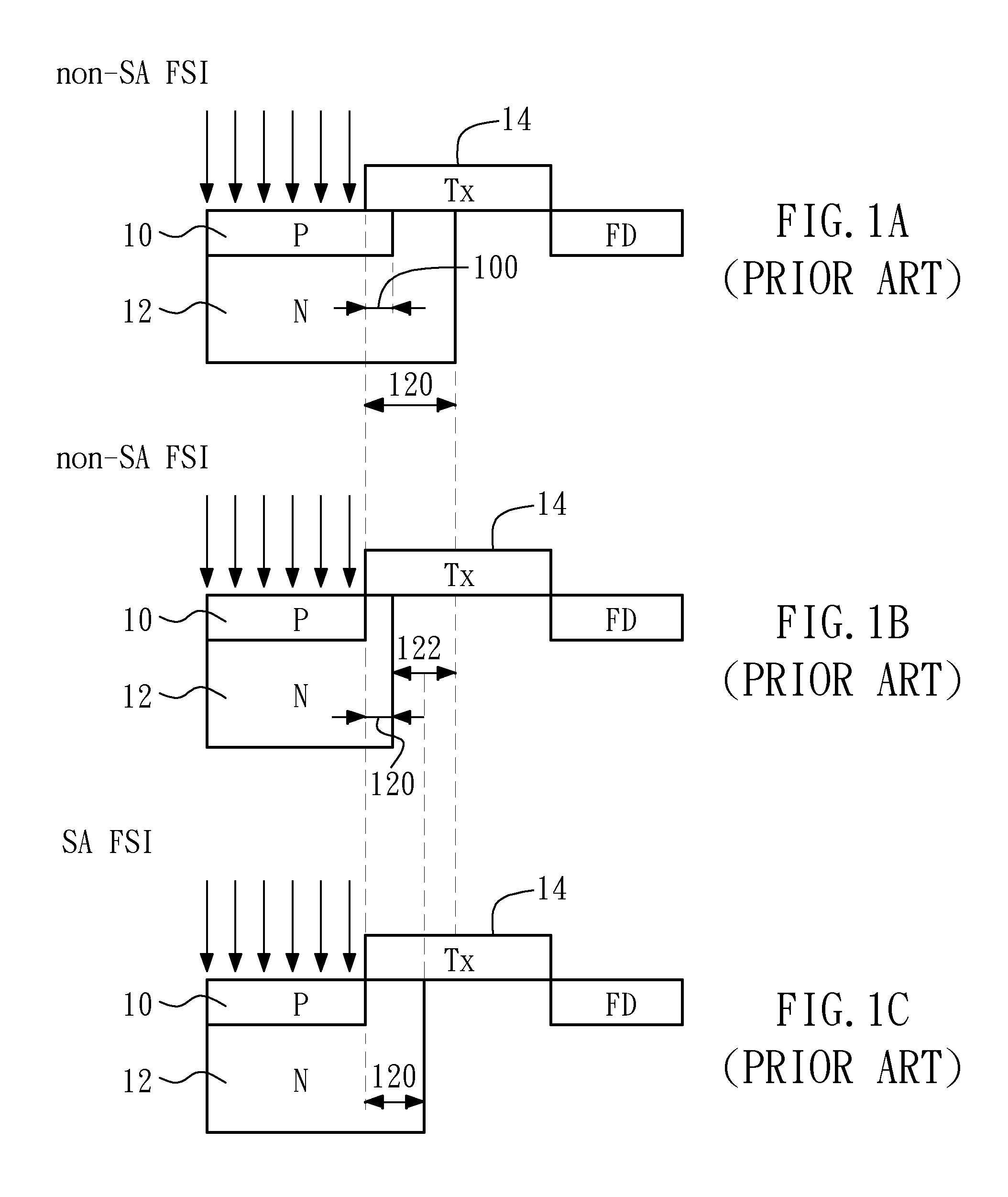
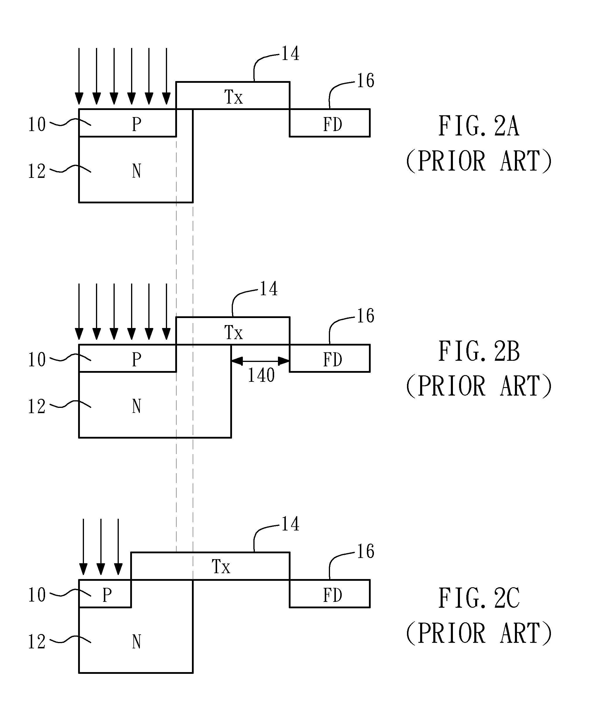
[0027]FIG. 3A to FIG. 3D show a sequence of cross sectional views that illustrates a process of forming a non-self aligned (non-SA) back side illumination (BSI) complementary metal oxide semiconductor (CMOS) image sensor (CIS) according to the present invention. It is noted that only layers or regions that are pertinent to the feature or features of the embodiment are discussed or shown. In other words, there may be further layer(s) or region(s) disposed between, on, below or adjacent to the shown layers or regions.

[0028]In FIG. 3A, all implants are within the top P type epitaxy portion of a semiconductor substrate 31 (e.g., a silicon substrate). A transfer gate (Tx) channel implant 30 such as p-type implant is formed in the semiconductor substrate 31. Subsequently, in FIG. 3B, an n-type doped region such as an n-type implant 32 is formed below the transfer gate channel implant 30. Next, in FIG. 3C, a thin gate oxide 37 is grown on the surface of substrate 31 and a transfer gate (Tx...

second embodiment

[0034]Moreover, the non-SA BSI CSI second embodiment can also benefit the burgeoning 3D CIS technology. It is shown in FIG. 6A a cross sectional view of the non-SA BSI CIS with extended transfer gate 33 at the pixel photo diode level along with circuit schematic of a portion of the pixel circuit (e.g., a reset transistor, a source follower SF and a select transistor SEL) at the pixel circuit level and two 3D vias 360 and 332 at FD 36 and Tx 33 respectively bridging the PD and Circuit levels in the vertical direction (the added 3rd dimension vs. the conventional 2D topology of Integrated Circuit). FIG. 6B shows a cross sectional view and circuit schematic of a counterpart without extended transfer gate. It is observed that the distance 330 between a transfer-gate 3D via 332 and a FD 3D via 360 may be substantially increased (compared to that shown in FIG. 6B), thereby reducing the coupling capacitance between them and thus increasing conversion gain.

[0035]The non-SA BSI CIS second em...


PUM


Abstract

A process and structure of a back side illumination (BSI) image sensor are disclosed. An n-type doped region is formed in a substrate, and a transfer gate is formed on top of the semiconductor substrate. A p-type doped region is formed in the n-type doped region either using the transfer gate as a mask or is non-self aligned formed.

Description

CROSS-REFERENCE TO RELATED APPLICATIONS[0001]This application claims the benefit of U.S. Provisional Application No. 61 / 294,398 (Att. Docket HI8351PR), filed Jan. 12, 2010 and entitled NON-SELF ALIGNED BACK SIDE ILLUMINATION (BSI) CMOS IMAGE SENSOR WITH AN EXTENDED TRANSFER GATE POLY, the entire contents of which are hereby incorporated by reference.BACKGROUND OF THE INVENTION[0002]1. Field of the Invention[0003]The present invention generally relates to an image sensor, and more particularly to a process and structure of a non-self aligned back side illumination (BSI) CMOS image sensor.[0004]2. Description of Related Art[0005]The pixel size of a complementary metal oxide semiconductor (CMOS) image sensor (CIS) becomes smaller than ever to meet high resolution and low form factor (or physical dimensions) requirement, for example, for mobile devices. FIG. 1A shows a cross sectional view of a conventional photodiode along with a portion of a pixel circuit. The front side of silicon wa...

Claims


Application Information

Patent Timeline
Patent Type & Authority Applications(United States)
IPC IPC(8): H01L31/10H01L31/18H01L31/0352
CPCH01L27/14614H01L27/14616H01L27/1464H01L27/14643H01L27/14687H01L27/14632
Inventor WU, YANGLIN, CHI-SHAO
Owner HIMAX IMAGING LIMITED
Why Eureka
Try Eureka