Display device

Inactive Publication Date: 2011-07-28
SEMICON ENERGY LAB CO LTD
View PDF45 Cites 39 Cited by
  • Summary
  • Abstract
  • Description
  • Claims
  • Application Information

AI Technical Summary

Benefits of technology

[0026]According to one embodiment of the present invention, a signal voltage applied to a pixel can be held stably by using a transistor whose off current is satisfactorily reduced. Consequently, a signal input to the pixel can be kept in a given state (the state in which an image signal is written), so that an image can be displayed stably.
[0027]According to one embodiment of the present invention, as a transistor provided in each pixel, a transistor whose channel formation region is formed using an oxide semiconductor layer is employed. When the oxide semiconductor layer is highly purified, off current of the transistor at room temperature can be lower than 10 zA/μm per micrometer of the channel width and off current of the transistor at 85° C. can be lower than 100 zA/μm per micrometer of the channel width. Therefore, the amount of leakage of an image signal through the transistor can be reduced. That is, display deterioration (change) which occurs when the writing fre

Problems solved by technology

Since operation speed of a thin film transistor using amorphous silicon is slow and any further high performance cannot be expected, a thin film transistor using polysilicon has be

Method used


Image

  • Display device
  • Display device
  • Display device

Examples


embodiment 1

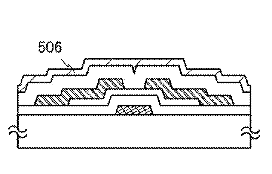
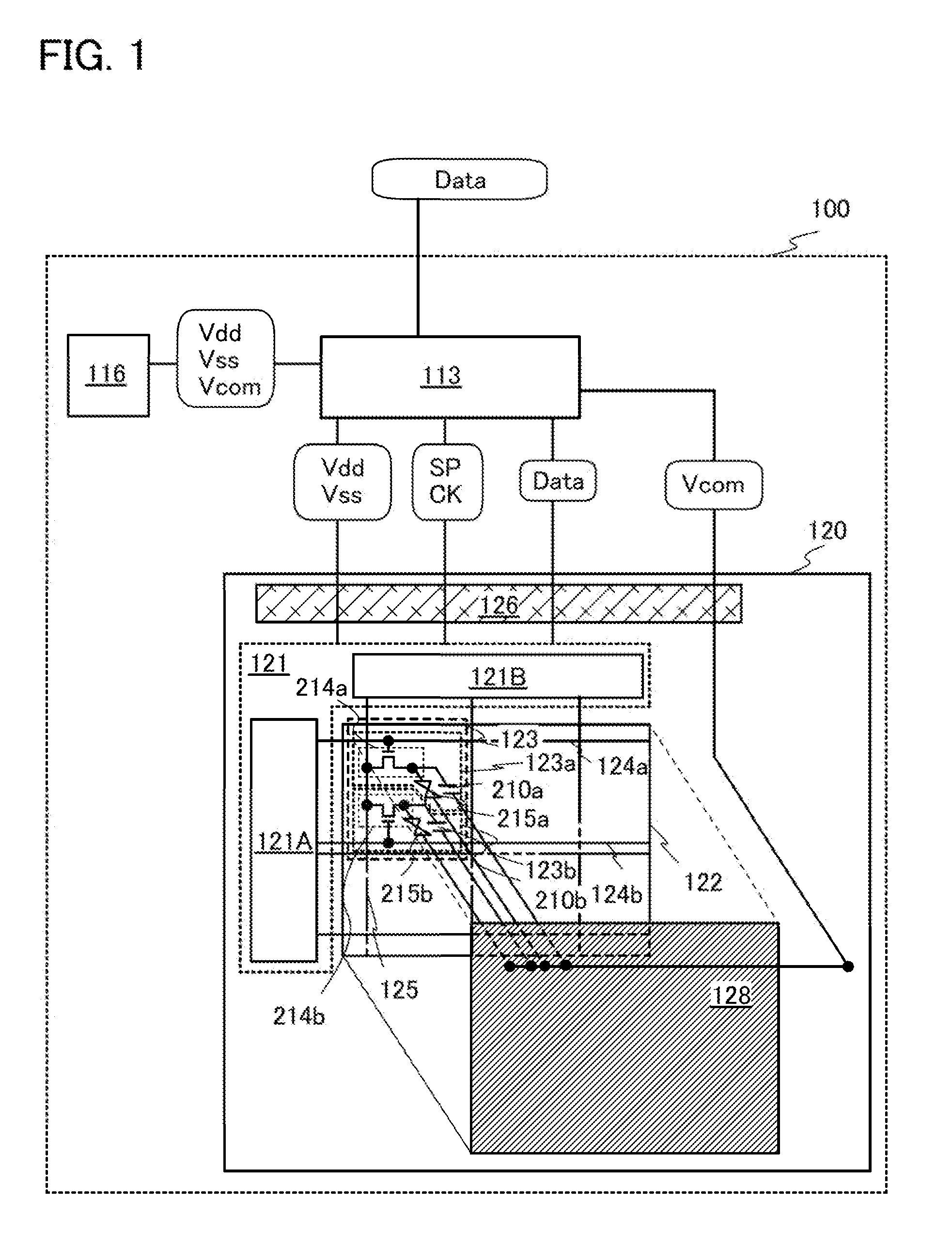
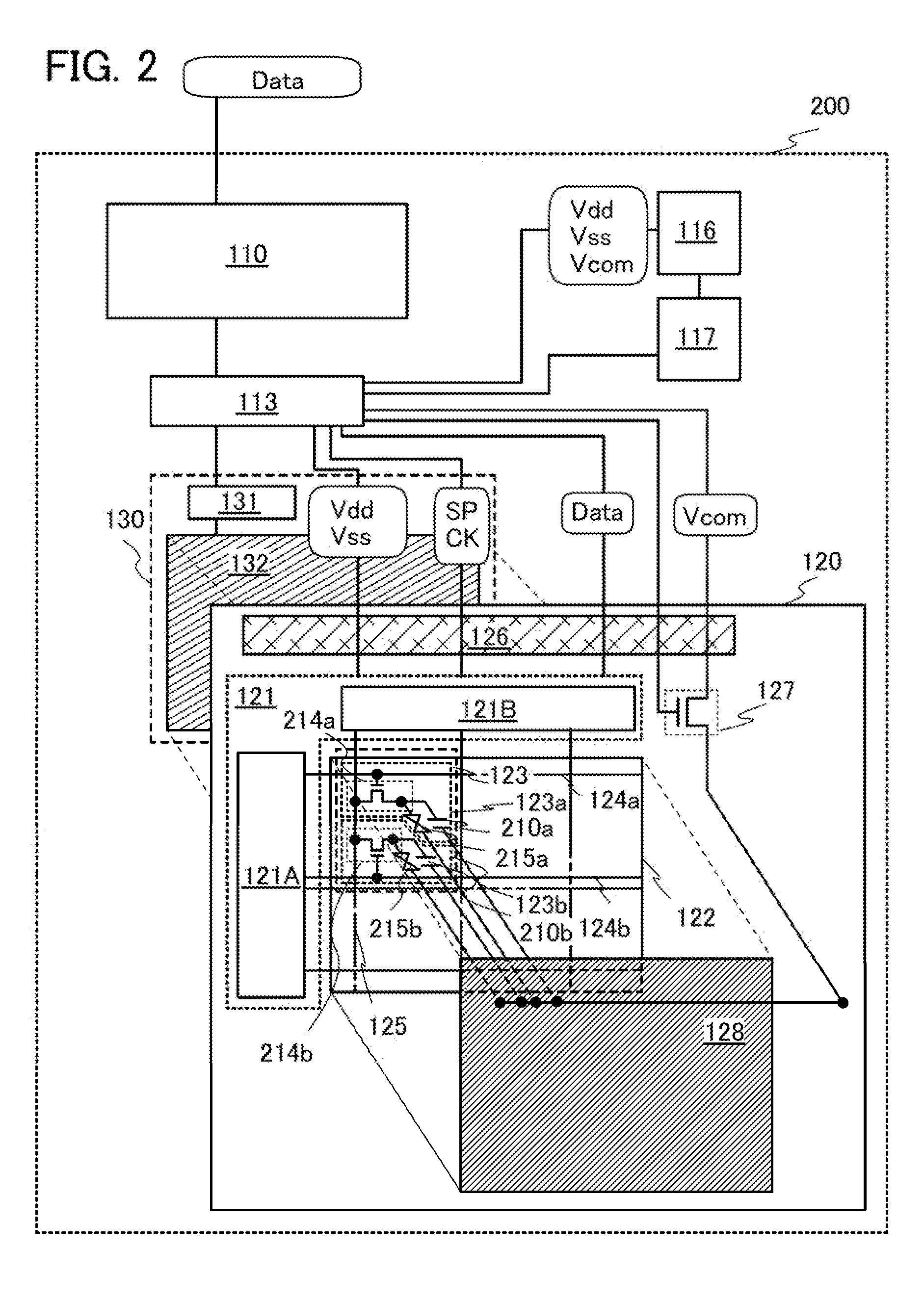
[0053]In this embodiment, one mode of a liquid crystal display device and a driving method of the liquid crystal display device are described with reference to FIG. 1, FIG. 2, FIG. 3, FIG. 4, FIGS. 5A and 5B, FIG. 6, and FIG. 7.

[0054]An example of each component of a liquid crystal display device 100 illustrated in this embodiment is described with reference to FIG. 1. The liquid crystal display device 100 includes a power supply 116, a display: control circuit 113, and a display panel 120. In the case of a transmissive liquid crystal display device or a transflective liquid crystal display device, a backlight portion which is one of lighting units may be further provided as a light source.

[0055]An image signal (image signal Data) is supplied to the liquid crystal display device 100 from an external device which is connected to the liquid crystal display device 100. Note that power supply potential (high power supply potential Vdd, low power supply potential Vss, and common potentia...

embodiment 2

[0139]In this embodiment, an example of an electronic device including the liquid crystal display device described in Embodiment 1 will be described.

[0140]FIG. 8A illustrates an external view of a television receiver which is an electronic device. FIG. 8A illustrates a housing 700 in which a display module 701 manufactured using the display panel described in Embodiment 1 is provided. The housing 700 includes a speaker 702, operation keys 703, an external connection terminal 704, an illuminance sensor 705, and the like.

[0141]The television receiver illustrated in FIG. 8A can display text information or a still image in addition to a moving image. A moving image can be displayed in a region of a display portion while a still image can be displayed in the other region. Note that a still image displayed includes characters, diagrams, signs, pictures, designs, and paintings or a combination of any of them. Alternatively, any of the displayed images which are colored is included.

[0142]FI...

embodiment 3

[0151]In this embodiment, description is made on a structure example of a backlight (a backlight portion, a backlight unit) which can be applied to a liquid crystal display device disclosed in this specification with reference to FIGS. 10A to 10C and FIGS. 11A to 11C.

[0152]FIG. 10A illustrates an example of a liquid crystal display device including a so-called edge-light type backlight portion 5201 and a display panel 5207. An edge-light type corresponds to a type in which a light source is provided at an end of a backlight portion and light of the light source is emitted from the entire light-emitting surface.

[0153]The backlight portion 5201 includes a diffusion plate 5202 (also referred to as a diffusion sheet), a light guide plate 5203, a reflection plate 5204, a lamp reflector 5205, and a light source 5206. Note that the backlight portion 5201 may also include a luminance improvement film or the like.

[0154]The light source 5206 has a function of emitting light as necessary. For ...


PUM


Abstract

A display panel for displaying an image is provided with a plurality of pixels arranged in a matrix. Each pixel includes one or more units each including a plurality of subunits. Each subunit includes a transistor in which an oxide semiconductor layer which is provided so as to overlap a gate electrode with a gate insulating layer interposed therebetween, a pixel electrode which drives liquid crystal connected to a source or a drain of the transistor, a counter electrode which is provided so as to face the pixel electrode, and a liquid crystal layer provided between the pixel electrode and the counter electrode. In the display panel, a transistor whose off current is lower than 10 zA/μm at room temperature per micrometer of the channel width and off current of the transistor at 85° C. can be lower than 100 zA/μm per micrometer in the channel width.

Description

TECHNICAL FIELD[0001]One embodiment of the present invention relates to a display device including a field-effect transistor using an oxide semiconductor.BACKGROUND ART[0002]A liquid crystal display panel including a thin film transistor using amorphous silicon as a driving element of liquid crystal is widely used in commercial products such as a monitor of a computer and a liquid crystal television. A manufacturing technique of a thin film transistor using amorphous silicon is already established and a liquid crystal panel with more than 60 inches has been produced.[0003]Since operation speed of a thin film transistor using amorphous silicon is slow and any further high performance cannot be expected, a thin film transistor using polysilicon has been developed. However, a crystallization step is required for making polysilicon, which leads to cause variation in transistor characteristics or inhibit enlargement of a panel area.[0004]In contrast, an oxide semiconductor material has b...

Claims


Application Information

Patent Timeline
IPC IPC(8): H01L29/12
CPCG02F1/13624H01L27/1225H01L27/3209H01L51/5024G02F1/136213G09G3/3648G09G2300/0809G02F1/133753H01L51/5278H10K59/32H10K50/12H10K50/19G02F1/1368G02F2202/10G09G2310/08H01L29/045H01L29/7869
Inventor YAMAZAKI, SHUNPEI
Owner SEMICON ENERGY LAB CO LTD
Why Eureka
Try Eureka