Electromigration immune through-substrate vias

a technology of electron immunodetection and through-substrat via, which is applied in the direction of semiconductor devices, semiconductor/solid-state device details, electrical apparatus, etc., can solve the problems of increasing electron scattering, metal ions to dislodge from the lattice and move physically, and metal lines or metal vias no longer provide a conductive path in the metal interconnect, etc., to achieve reliable electrical connection

Active Publication Date: 2011-08-11
IBM CORP
View PDF128 Cites 55 Cited by
  • Summary
  • Abstract
  • Description
  • Claims
  • Application Information

AI Technical Summary

Benefits of technology

[0009]A through-substrate via (TSV) structure is provided that includes at least two electrically conductive via segments embedded in a substrate. The at least two electrically conductive via segments are separated from each other by an electrically conductive barrier layer therebetween. The length of each individual conductive via segment is typically equal to, or less than, the Blech length of the conductive material so that the stress-induced back flow force, generated by each conductive barrier layer, cancels the electromigration force in each conductive via segment. Consequently, the TSV structures are immune to electromigration, and provide reliable electrical connections among chips stacked in 3 dimensions.

Problems solved by technology

High defect density, i.e., smaller grain size of the metal, or high temperature typically increases electron scattering.
Such momentum transfer, if performed sufficiently cumulatively, may cause the metal ions to dislodge from the lattice and move physically.
Such a void results in a locally increased resistance in the metal interconnect, or even an outright circuit “open.” In this case, the metal line or the metal via no longer provides a conductive path in the metal interconnect.
Formation of voids in the metal line or the metal via can thus result in a product failure in semiconductor devices.
Further, accumulation of electromigrated materials as extrusions or hillocks outside the volume of the original metal structures can result in electrical “shorts” with adjacent metal structures.
Thus, the TSVs as known in the prior art are inherently subject to electromigration, and can fail during operation of the semiconductor chips.

Method used


Image

  • Electromigration immune through-substrate vias
  • Electromigration immune through-substrate vias
  • Electromigration immune through-substrate vias

Examples


first embodiment

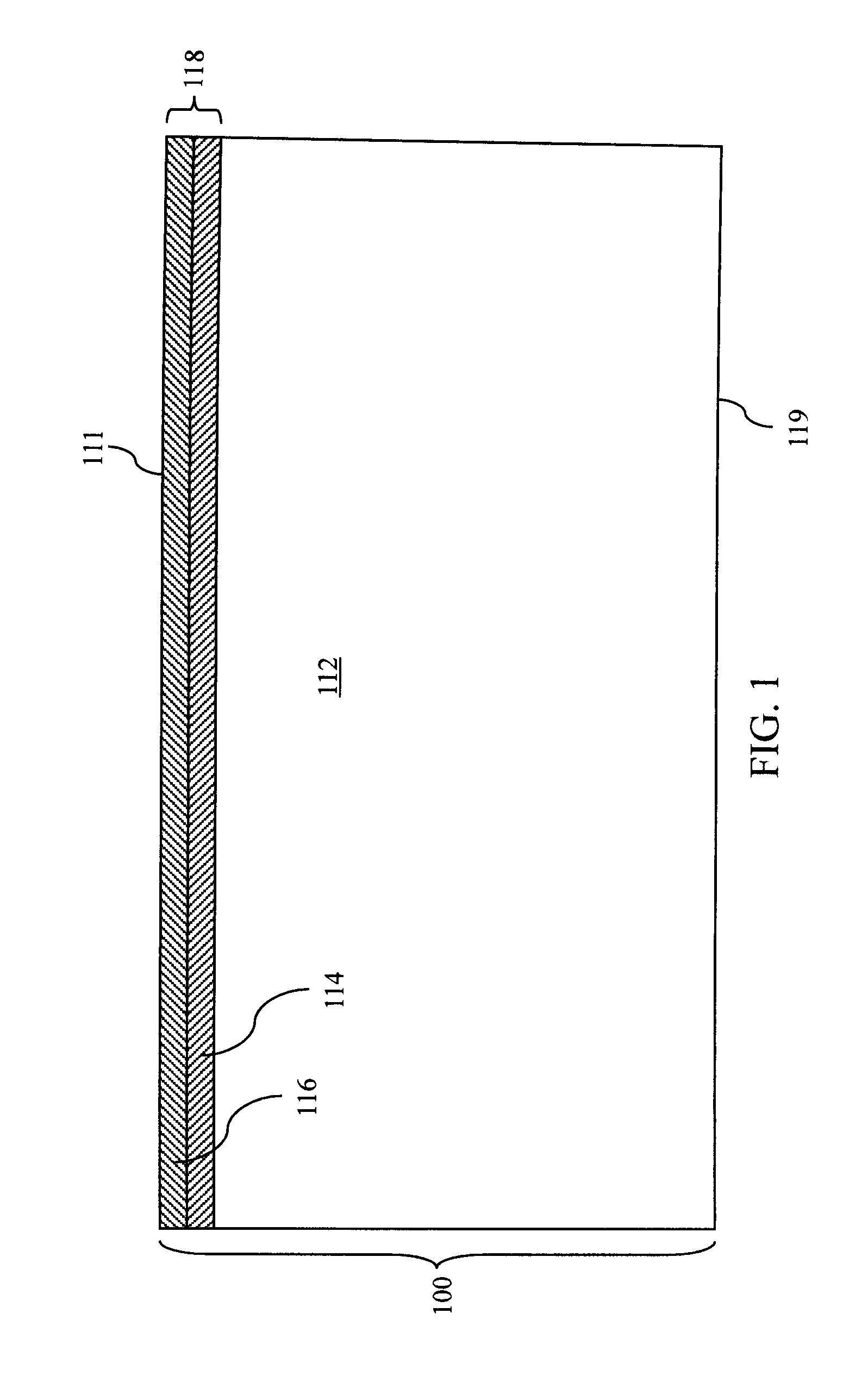
[0028]Referring to FIG. 1, a first exemplary semiconductor structure according to the present invention includes a first substrate 100. The first substrate 100 can include a first handle substrate 112 and a first semiconductor-device-containing layer 118 that can include at least one semiconductor device such as a field effect transistor, a bipolar transistor, a diode, a thyristor, and a memory cell. The first semiconductor-device-containing layer 118 can include semiconductor devices for a semiconductor chip. The first substrate 100 typically has a first substantially planar surface 111 on one side and a second substantially planar surface 119 on an opposite side. The thickness of the first substrate 100 is typically from 100 microns to 1,000 microns, although lesser and greater thicknesses can also be employed.

[0029]A lower portion of the first semiconductor-device-containing layer 118 can include a semiconductor material layer 114. The semiconductor material layer 114 includes a ...

second embodiment

[0068]Referring to FIG. 11, a second exemplary semiconductor structure according to the present invention is derived from the first exemplary semiconductor structure by employing a second substrate 200 including at least another TSV structure 280, which can be a second plurality of TSV structures. The second plurality of TSV structures 280 in the second substrate 200 can be formed employing the same processing steps as illustrated in FIGS. 2-9. Each of the at least another TSV structure 280 extends from the third substantially planar surface 211 to a fourth substantially planar surface 219 that are located on opposite sides second substrate 200. Each of the at least another TSV structure 280 includes another plurality of conductive via segments that are vertically spaced from one another by at least another conductive liner portion. The at least another TSV structure 280 in the second substrate 200 is formed before forming the second BEOL metal interconnect layer 290 and bonding of ...

third embodiment

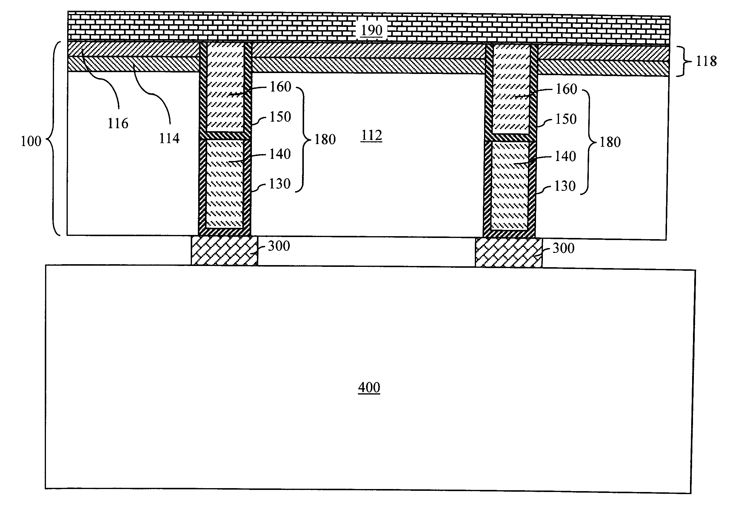
[0070]Referring to FIG. 12, a third exemplary semiconductor structure according to the present invention is derived from the first exemplary semiconductor structure by employing a packaging substrate 400 instead of a second substrate 200. The packaging substrate 400 can be a ceramic substrate or a laminar substrate comprising a dielectric material.

[0071]The array of conductive bonding material structures 300 provides a plurality of electrical connections between the at least one semiconductor device in the first semiconductor-device-containing layer 118 and the conductive structures located in the packaging substrate 400 to provide three-dimensional chip integration.

[0072]Further, any mounting structure can be employed instead of a second substrate 200 or a packaging substrate to provide a three-dimensional integration of semiconductor chips as needed. Because the length of each conductive via segment does not exceed the Blech length, each of the at least one TSV structure 180 and t...


PUM


Abstract

A through-substrate via (TSV) structure includes at least two electrically conductive via segments embedded in a substrate and separated from each other by an electrically conductive barrier layer therebetween. The length of each individual conductive via segment is typically equal to, or less than, the Blech length of the conductive material so that the stress-induced back flow force, generated by each conductive barrier layer, cancels the electromigration force in each conductive via segment. Consequently, the TSV structures are immune to electromigration, and provide reliable electrical connections among a chips stacked in 3 dimensions.

Description

BACKGROUND[0001]The present invention relates to the field of semiconductor structures, and particularly to electromigration immune through-substrate vias and methods of manufacturing the same.[0002]A metal structure includes a lattice of metal ions and non-localized free electrons. The metal ions are formed from metal atoms that donate some of their electrons to a common conduction band of the lattice, and the non-localized free electrons move with relatively small resistance within the lattice under an electric field. Normal metal lines, excluding superconducting materials at or below a superconducting temperature, have finite conductivity, which is caused by interaction of electrons with crystalline imperfections and phonons which are thermally induced lattice vibrations.[0003]When electrical current flows in the metal line, the metal ions are subjected to an electrostatic force due to the charge of the metal ion and the electric field to which the metal ion is exposed to. Furthe...

Claims


Application Information

Patent Timeline
Patent Type & Authority Applications(United States)
IPC IPC(8): H01L23/48H01L21/50
CPCH01L21/76898H01L2924/0002H01L24/16H01L25/0657H01L2224/13025H01L2225/06513H01L2225/06541H01L2924/01078H01L2924/01079H01L2924/04941H01L2224/9202H01L2924/10253H01L24/13H01L2924/00014H01L2924/1305H01L2924/1301H01L2224/0401H01L2224/0557H01L2924/00H01L2224/05552H01L24/03H01L24/05
Inventor FILIPPI, RONALD G.FITZSIMMONS, JOHN A.KOLVENBACH, KEVINWANG, PING-CHUAN
Owner IBM CORP
Why Eureka
Try Eureka