Memory component, memory device, and method of operating memory device

a memory component and memory device technology, applied in semiconductor devices, digital storage, instruments, etc., can solve the problems of insufficient erasure performance, and insufficient resistance separation width between the resistance value in the written state and the resistance value in the erased state. , to achieve the effect of reducing resistance, preventing an unnecessary oxidation reaction, and improving the repeatability of the effect of durability

Inactive Publication Date: 2011-08-11
SONY SEMICON SOLUTIONS CORP
View PDF1 Cites 133 Cited by
  • Summary
  • Abstract
  • Description
  • Claims
  • Application Information

AI Technical Summary

Benefits of technology

[0017]In this specification, since the resistance variable layer contains the aluminum oxide and at least one of the transition metal oxide and the transition metal oxynitride having a lower resistance than the aluminum oxide, even when the voltage or current pulse of the positive direction is applied to the memory component, it is difficult for a voltage bias to be applied to the transition metal oxide or the transition metal oxynitride. Therefore, even when the memory component is in the written state (low-resistance state), the transition metal oxide or the transition metal oxynitride is not reduced but forms an oxide film or an oxynitride film on the first electrode. Therefore, it is possible to prevent an unnecessary oxidation reaction between the first electrode and the chalcogen element contained in the ion source layer from occurring in response to repeated write and erase operations.
[0018]According to the memory component or the memory device of the embodiment of the present invention, since the resistance variable layer contains the aluminum oxide and at least one of a transition metal oxide and a transition metal oxynitride having a lower resistance than the aluminum oxide, it is possible to improve the repetition durability thereof.
[0019]According to the method of operating the memory device of the embodiment of the present invention, when a voltage is applied between a first electrode and a second electrode, in an ion source layer, aluminum (Al) ions and ions of a metal element contained in the ion source layer are moved towards the first electrode side, and in a resistance variable layer, a conduction path is formed by a reduction reaction of an aluminum oxide or the ions of the metal element, thus realizing a low-resistance state. Moreover, when a reverse polarity voltage is applied between the first electrode and the second electrode, in the ion source layer, the aluminum (Al) ions and the ions of the metal element contained in the ion source layer are moved towards the second electrode side, and in the resistance variable layer, the aluminum (Al) ions form an aluminum oxide through an oxidation reaction, thus realizing a high-resistance state, or the reduced metal element is ionized to move towards the ion source layer, thus destroying the conduction path and realizing a high-resistance state. Therefore, it is possible to improve the repetition durability of the memory device.

Problems solved by technology

However, the configuration disclosed in JP-A-2005-197634 has an insufficient erasure performance, and when a number of bits are rewritten, the resistance value in the erased state tends to shift towards the lower side.
Thus, a resistance separation width between the resistance value in the written state and the resistance value in the erased state is not sufficient, and there is room for improvement in repetition durability.

Method used


Image

  • Memory component, memory device, and method of operating memory device
  • Memory component, memory device, and method of operating memory device
  • Memory component, memory device, and method of operating memory device

Examples


first embodiment

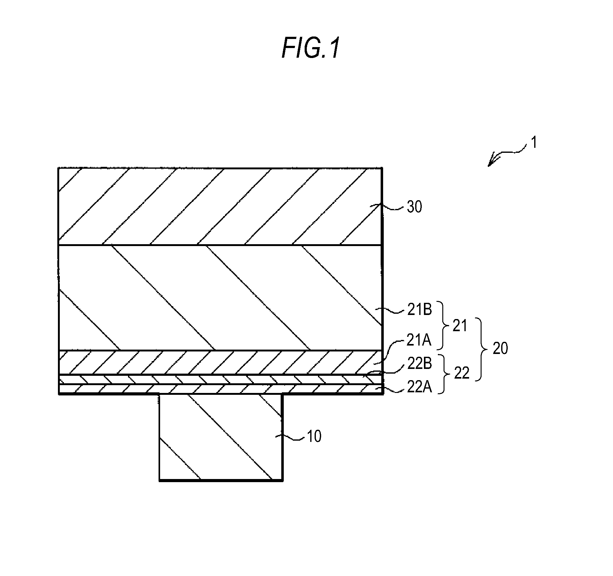
[0084]FIG. 1 is a cross-sectional view showing a configuration of a memory component 1 according to a first embodiment of the present invention. The memory component 1 includes a lower electrode 10 (first electrode), a memory layer 20, and an upper electrode 30 (second electrode) which are provided in that order. The memory layer 20 includes an ion source layer 21 and a resistance variable layer 22 which are provided in that order from the side of the upper electrode 30.

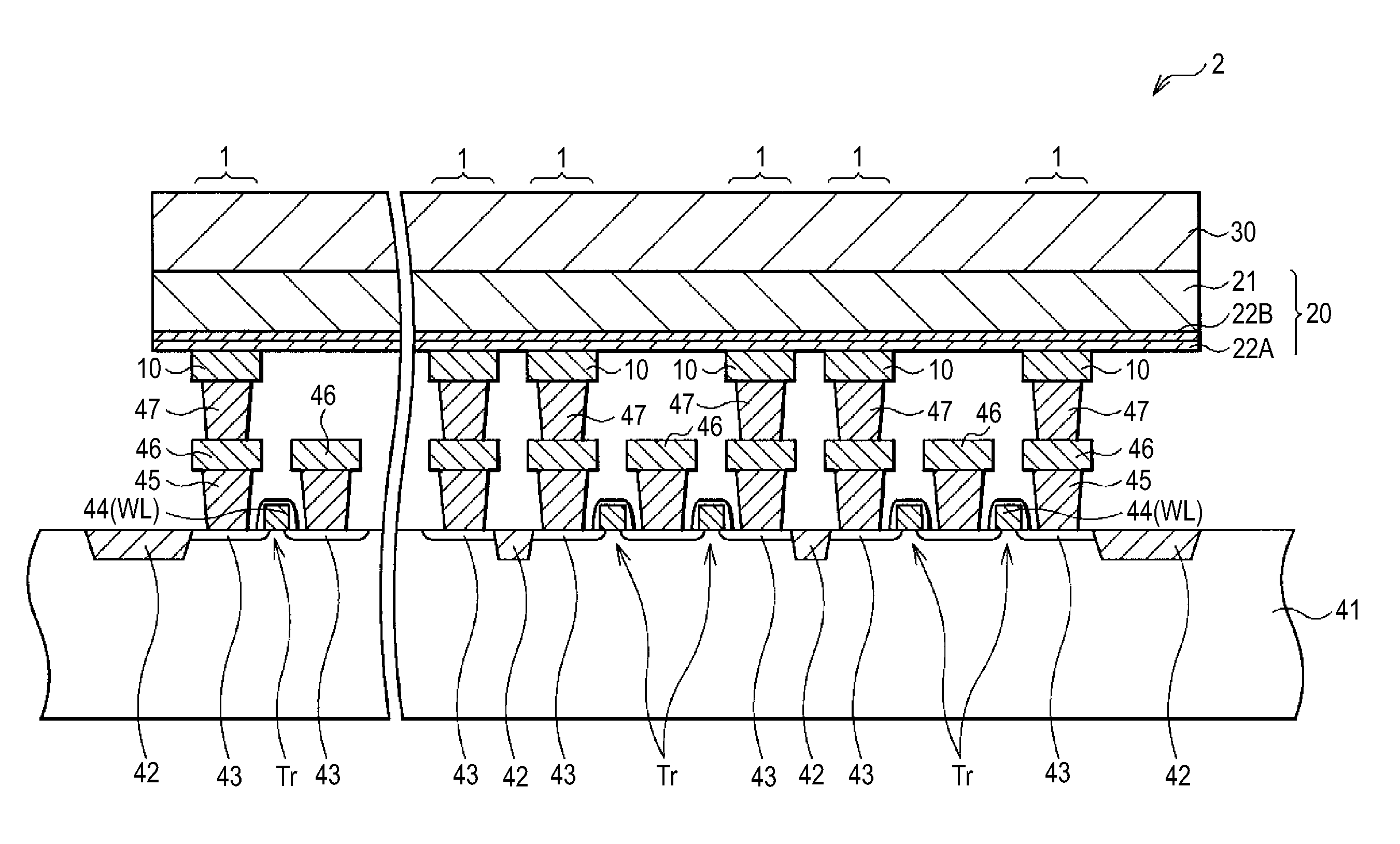
[0085]The lower electrode 10 is provided on a silicon substrate 41 on which a CMOS (Complementary Metal Oxide Semiconductor) circuit, for example, is formed as described later (see FIG. 13), and serves as a connection portion to the CMOS circuit portion. The lower electrode 10 is formed of a wiring material used in the semiconductor process, such as, for example, tungsten (W), tungsten nitride (WN), copper (Cu), aluminum (Al), Molybdenum (Mo), tantalum (Ta), and silicide. When the lower electrode 10 is formed of a ma...

modification 1

(Modification 1)

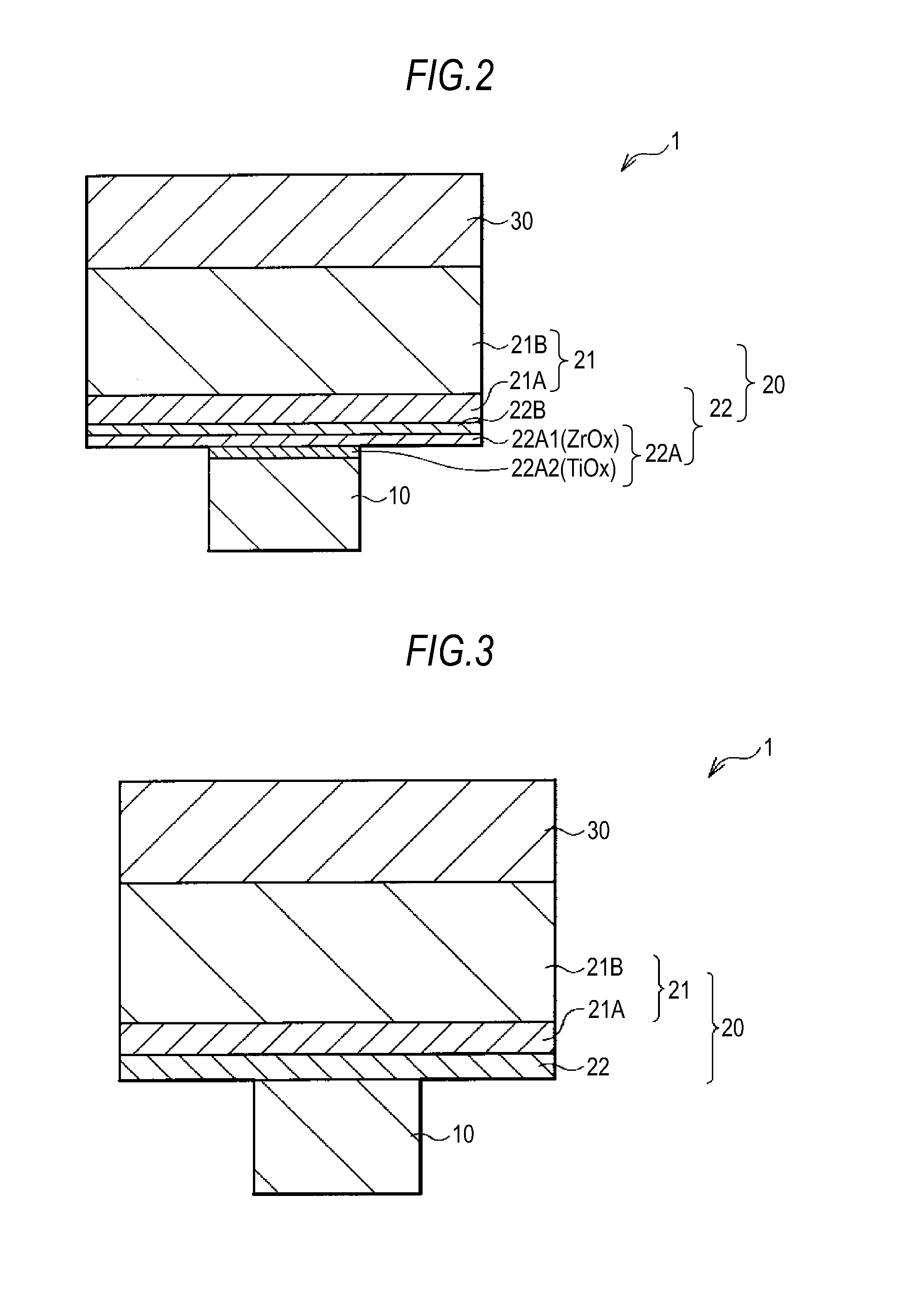
[0147]In the embodiment described above, a case where the resistance variable layer 22 has a configuration in which the first layer 22A made of the transition metal oxide and the second layer 22B containing the aluminum oxide as its main component are laminated in that order from the side of the lower electrode 10 has been described. However, the resistance variable layer 22 may have a single-layered structure in which the aluminum oxide and the transition metal oxide are contained in a mixed state as shown in FIG. 3.

[0148]In this case, when a positive voltage is applied to the memory component 1 so that the upper electrode 30 is on the positive potential side and the lower electrode 10 is on the negative potential side, for example, in the ion source layer 21, the Al ions and the ions of the metal element contained in the ion source layer 21 are moved towards the lower electrode 10 side. In this case, on the lower electrode 10, a conduction path is formed by the red...

modification 2

(Modification 2)

[0150]In the embodiment described above, a case where the ion source layer 21 has the two-layered structure of the intermediate layer 21A and the ion supply layer 21B has been described. However, the ion source layer 21 does not necessarily have the intermediate layer 21A but may have a single-layered structure of only the ion supply layer 21B as shown in FIG. 4.


PUM


Abstract

A memory component includes: a first electrode; a memory layer; and a second electrode which are provided in that order, wherein the memory layer includes an ion source layer containing aluminum (Al) together with at least one chalcogen element selected from the group consisting of tellurium (Te), sulfur (S), and selenium (Se), and a resistance variable layer provided between the ion source layer and the first electrode and containing an aluminum oxide and at least one of a transition metal oxide and a transition metal oxynitride having a lower resistance than the aluminum oxide.

Description

BACKGROUND OF THE INVENTION[0001]1. Field of the Invention[0002]The present invention relates to a memory component and a memory device capable of storing information using a change in electrical characteristics of a memory layer that includes an ion source layer and a resistance variable layer, and a method of operating a memory device.[0003]2. Description of the Related Art[0004]In information equipment such as a computer, high-speed and high-density DRAMs (Dynamic Random Access Memory) have been widely used as a random access memory. However, DRAMs involve high manufacturing costs due to their complicated manufacturing process as compared to typical logic circuit LSIs and signal processing circuits used in electronic equipment. Moreover, DRAMs are volatile memories in which information is lost when power is turned off. Therefore, it is necessary for DRAMs to perform a frequent refresh operation; that is, the written information (data) must be read, amplified again and rewritten.[...

Claims


Application Information

Patent Timeline
Patent Type & Authority Applications(United States)
IPC IPC(8): G11C11/00H01L45/00
CPCG11C13/0011H01L27/2436H01L27/2472H01L45/085H01L45/1253H01L45/145H01L45/146H01L45/1633H01L45/1266G11C11/161H10B63/82H10B63/30H10N70/245H10N70/8416H10N70/826H10N70/883H10N70/8833H10N70/028G11C2213/51H10N70/841G11C11/16
Inventor OHBA, KAZUHIROYASUDA, SHUICHIROMIZUGUCHI, TETSUYAARATANI, KATSUHISASHIMUTA, MASAYUKIKOUCHIYAMA, AKIRAOGASAWARA, MAYUMI
Owner SONY SEMICON SOLUTIONS CORP
Why Eureka
Try Eureka